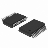
TDA9884TS/V1,112 NXP Semiconductors, TDA9884TS/V1,112 Datasheet - Page 36

TDA9884TS/V1,112
Manufacturer Part Number
TDA9884TS/V1,112
Description
IC IF-PLL I2C-BUS DEMOD 24-SSOP
Manufacturer
NXP Semiconductors
Type
Demodulatorr
Datasheet
1.TDA9884TSV1112.pdf
(58 pages)
Specifications of TDA9884TS/V1,112
Package / Case
*
Applications
Mobile Reception
Mounting Type
Surface Mount
Maximum Operating Temperature
+ 70 C
Minimum Operating Temperature
- 20 C
Mounting Style
SMD/SMT
Lead Free Status / RoHS Status
Lead free / RoHS Compliant
Other names
935270308112
TDA9884TS/V1
TDA9884TS/V1
TDA9884TS/V1
TDA9884TS/V1
Philips Semiconductors
[5]
[6]
[7]
[8]
[9]
[10] The intermodulation figures are defined for:
[11] Measurements taken with SAW filter M1963M (sound shelf: 20 dB); loop bandwidth BL = 70 kHz. Modulation VSB; sound carrier off;
[12] Measurements taken with SAW filter M1963M (sound shelf: 20 dB); loop bandwidth BL = 70 kHz. Sound carrier on;
[13] AC load; C
[14] The sound carrier trap can be bypassed by switching the I
[15] If selected by the I
[16] The response time is valid for a VIF input level range from 200 V to 70 mV.
[17] The fast mode will be activated automatically, if within a time of typically 150 s for mobile mode and 1.2 ms for normal mode no AGC
[18] The fast mode will be activated automatically, if the black level drops down by half of the sync amplitude.
[19] If selected by the I
[20] Pin AFC is usable as AFC output or as SIF-AGC.
[21] The tolerance of the reference frequency determines the accuracy of the VIF-AFC, FM demodulator center frequency and maximum
[22] The intercarrier output signal at pin SIOMAD can be calculated by the following formulae taking into account the internal video signal
[23] For normal operation (with the I
[24] SIF input level is 10 mV (RMS); VIF input level is 10 mV (RMS) unmodulated.
TDA9884_2
Product data sheet
Loop bandwidth BL = 70 kHz (damping factor d = 1.9; calculated with sync level within gain control range). Calculation of the VIF-PLL
filter can be done by use of the following formulae:
steepness
loop bandwidth for 3 dB; d is the damping factor.
V
Condition: luminance range (5 steps) from 0 % to 100 %.
Measurement using unified weighting filter (“ ITU-T J.61” ), 200 kHz high-pass filter, 5 MHz low-pass filter and subcarrier notch filter
(“ ITU-T J.64” ).
Noise analyzer setting: 200 kHz high-pass and SC-trap switched on.
a) f = 1.1 MHz (referenced to black and white signal) as
b) f = 3.3 MHz (referenced to color carrier) as
f
f
carrier traps (see
The amplitude is 1.1 V (p-p).
function.
event occurs. An AGC event is a charge current pulse into the AGC capacitor due to reaching AGC reference voltage the sync level.
cannot be used for the normal port function.
a) To match the AFC output signal to different tuning systems a current source output is provided. The test circuit is given in
b) In mobile mode the internal SIF-AGC is switched to pin AFC. In this case AFC out is disabled.
FM deviation.
with 1.1 V (p-p) as a reference:
the correction term for RMS value,
term of internal circuitry and 3 dB is the tolerance of video output and intercarrier output V
the application of a 2.2 k resistor between pin SIOMAD and ground. If this MAD2 is activated, also the power-on setup state activates
a VIF frequency of 58.75 MHz.
video
video
i(VIF)
The AFC steepness can be changed by resistors R1 and R2.
> 0.5 MHz.
= 10 kHz to 10 MHz.
= 10 mV (RMS); f = 1 MHz (VCO frequency offset related to picture carrier frequency); white picture video modulation.
L
rad
-------- -
< 20 pF and R
V
Figure 16
2
2
or
C-bus, the VIF-AGC voltage can be monitored at pin OP2. In this case, OP2 cannot be used for the normal port
C-bus, pin OP1 can alternatively be used for external AGC control, activated by pin AGCSW. In this case, OP1
2
------ -
Hz
V
L
to
> 1 k . The sound carrier frequencies (depending on TV standard) are attenuated by the integrated sound
; K
Figure
2
V
C-bus) no DC load at pin SIOMAD is allowed. The second module address (MAD2) will be activated by
D
o intc rms
is the phase detector steepness
--------------- - dB
V
V
i PC
i SC
21; H (s) is the absolute value of transfer function).
=
IM
is the sound-to-picture carrier ratio at pins VIF1 and VIF2 in dB, 6 dB is the correction
1.1
BL
=
Rev. 02 — 12 May 2006
-3dB
--------- -
2 2
20 log
1
2
IM
C-bus. In this way the full composite video spectrum appears at pin CVBS.
=
I
----- -K
2
10
2
1
=
V
------------------------------------- - .
V
C-bus controlled multistandard alignment-free IF-PLL
r
0
0
20 log
V
O
at 4.4 MHz
at 3.3 MHz
K
-------- -
rad
and
D
A
R
V
------------------------------------- -
V
, valid for d
r
; R is the loop resistor; C is the loop capacitor; BL
0
0
=
at 4.4 MHz
at 1.1 MHz
----- -
20
1
--------------- - dB
V
V
1.2;
i SC
i PC
o(intc)(rms)
+
d
3.6 dB.
=
© Koninklijke Philips Electronics N.V. 2006. All rights reserved.
1
-- - R K
2
.
+
6 dB 3 dB
O
K
D
C
TDA9884
, where: K
, where:
O
is the VCO
Figure
3dB
--------- -
2 2
36 of 58
1
is the
is
7.


