XE8000EV120 Semtech, XE8000EV120 Datasheet - Page 4
XE8000EV120
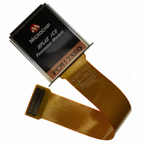
Manufacturer Part Number
XE8000EV120
Description
BOARD EVAL FOR SX8722I070TRLF
Manufacturer
Semtech
Series
ZoomingADC™r
Specifications of XE8000EV120
Number Of Adc's
1
Number Of Bits
16
Data Interface
I²C
Inputs Per Adc
7 Single or 4 Differential
Voltage Supply Source
Single Supply
Operating Temperature
-40°C ~ 125°C
Utilized Ic / Part
SX8722
Lead Free Status / RoHS Status
Lead free / RoHS Compliant
Other names
XM8000EV120
XM8000EV120
XM8000EV120


Section
12.
ACS - Revision 4.2
©2008 Semtech Corp.
ADVANCED COMMUNICATIONS & SENSING
Table of contents
11.7. Using the SX8722 Stand alone...................................................................................................................... 47
11.8. Frequency calibration process ....................................................................................................................... 48
11.9. Working below 3 V ......................................................................................................................................... 50
12.1. ZoomingADC Features .................................................................................................................................. 51
12.2. Acquisition Chain ........................................................................................................................................... 51
12.3. ZoomingADC Detailed block diagram............................................................................................................ 53
12.4. ZoomingADC register map ............................................................................................................................ 54
12.5. ZoomingADC™ registers table ...................................................................................................................... 56
12.6. Input Multiplexers........................................................................................................................................... 57
12.7. Programmable Gain Amplifiers ...................................................................................................................... 58
12.8. ADC Characteristics....................................................................................................................................... 62
12.9. Power Saving Modes ..................................................................................................................................... 69
12.10. Input impedance............................................................................................................................................ 69
12.11. Switched Capacitor Principle......................................................................................................................... 70
12.12. PGA Settling or Input Channel Modifications ................................................................................................ 71
12.13. PGA Gain & Offset, Linearity and Noise ....................................................................................................... 71
12.14. Power Reduction ........................................................................................................................................... 71
12.15. Noise ............................................................................................................................................................. 72
12.16. Gain Error and Offset Error ........................................................................................................................... 73
ZoomingADC ......................................................................................................................................................... 51
12.8.1. Conversion Sequence............................................................................................................................. 62
12.8.2. Sampling Frequency ............................................................................................................................... 63
12.8.3. Over-Sampling Ratio............................................................................................................................... 63
12.8.4. Elementary Conversions......................................................................................................................... 64
12.8.5. Resolution ............................................................................................................................................... 64
12.8.6. Conversion Time & Throughput .............................................................................................................. 65
12.8.7. Output Code Format ............................................................................................................................... 67
11.7.1. Schematic ............................................................................................................................................... 47
11.8.1. Overview ................................................................................................................................................. 48
11.8.2. Using an 32.768 kHz XTAL..................................................................................................................... 48
11.8.3. Using a 32.768 kHz External clock source ............................................................................................. 49
11.9.1. Operating range ...................................................................................................................................... 50
11.9.2. Internal voltage multiplier ........................................................................................................................ 50
11.9.3. Schematic ............................................................................................................................................... 50
12.1.1. Overview ................................................................................................................................................. 51
12.7.1. PGA & ADC Enabling ............................................................................................................................. 58
12.7.2. PGA1 ...................................................................................................................................................... 58
12.7.3. PGA2 ...................................................................................................................................................... 59
12.7.4. PGA3 ...................................................................................................................................................... 60
October 2008
Page 4
High gain acquisition for sensor interface
DATASHEET
www.semtech.com
SX8722
Page
Related parts for XE8000EV120
Image
Part Number
Description
Manufacturer
Datasheet
Request
R

Part Number:
Description:
EVALUATION BOARD
Manufacturer:
Semtech
Datasheet:
Part Number:
Description:
EVALUATION BOARD
Manufacturer:
Semtech
Datasheet:
Part Number:
Description:
VOLTAGE SUPPRESSOR, TRANSIENT SEMTECH
Manufacturer:
Semtech
Datasheet:

Part Number:
Description:
HIGH VOLTAGE CAPACITORS MONOLITHIC CERAMIC TYPE
Manufacturer:
Semtech Corporation
Datasheet:
Part Number:
Description:
EZ1084CM5.0 AMP POSITIVE VOLTAGE REGULATOR
Manufacturer:
Semtech Corporation
Datasheet:
Part Number:
Description:
3.0 AMP LOW DROPOUT POSITIVE VOLTAGE REGULATORS
Manufacturer:
Semtech Corporation
Datasheet:
Part Number:
Description:
Manufacturer:
Semtech Corporation
Datasheet:
Part Number:
Description:
RailClamp Low Capacitance TVS Diode Array
Manufacturer:
Semtech Corporation
Datasheet:
Part Number:
Description:
Manufacturer:
Semtech Corporation
Datasheet:
Part Number:
Description:
Manufacturer:
Semtech Corporation
Datasheet:
Part Number:
Description:
Manufacturer:
Semtech Corporation
Datasheet:
Part Number:
Description:
Manufacturer:
Semtech Corporation
Datasheet: