XE8000EV120 Semtech, XE8000EV120 Datasheet - Page 9
XE8000EV120
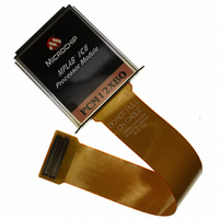
Manufacturer Part Number
XE8000EV120
Description
BOARD EVAL FOR SX8722I070TRLF
Manufacturer
Semtech
Series
ZoomingADC™r
Specifications of XE8000EV120
Number Of Adc's
1
Number Of Bits
16
Data Interface
I²C
Inputs Per Adc
7 Single or 4 Differential
Voltage Supply Source
Single Supply
Operating Temperature
-40°C ~ 125°C
Utilized Ic / Part
SX8722
Lead Free Status / RoHS Status
Lead free / RoHS Compliant
Other names
XM8000EV120
XM8000EV120
XM8000EV120


Notes
(1)
(2)
(3)
(4)
(5)
(6)
(7)
(8)
(9)
(10)
(11)
(12)
(13)
(14)
(15)
(16)
(17)
(18)
(19)
ACS - Revision 4.2
©2008 Semtech Corp.
ADVANCED COMMUNICATIONS & SENSING
Gain defined as overall PGA gain GDTOT = GD1 x GD2 x GD3. Maximum input voltage is given by:
V
Offset due to tolerance on GDoff2 or GDoff3 setting. For small intrinsic offset, use only ADC and PGA1.
Measured with block connected to inputs through AMUX block. Normalized input sampling frequency for input impedance is f
512 kHz. This figure must be multiplied by 2 for f
Figure independent from PGA1 gain and sampling frequency f
Figure independent on PGA2 gain and sampling frequency f
Figure independent on PGA3 gain and sampling frequency f
Resolution is given by n = 2 log
set to 1, 2, 4 or 8.
If a ramp signal is applied to the input, all digital codes appear in the resulting ADC output data.
Gain error is defined as the amount of deviation between the ideal (theoretical) transfer function and the measured transfer
function (with the offset error removed).
Offset error is defined as the output code error for a zero volt input (ideally, output code = 0). For 1 LSB offset, N
2.
INL defined as the deviation of the DC transfer curve of each individual code from the best-fit straight line. This specification holds
over the full scale.
DNL is defined as the difference (in LSB) between the ideal (1 LSB) and measured code transitions for successive codes.
Values for Gains = 1 to 100. PSRR is defined as the amount of change in the ADC output value as the power supply voltage
changes.
Conversion time is given by: T
N
PGAs are reset after each writing operation to registers CxRegAdc1-5. The ADC must be started after a PGA or inputs common-
mode stabilisation delay. This is done by writing bit Start several cycles after PGA settings modification or channel switching.
Delay between PGA start or input channel switching and ADC start should be equivalent to OSR (between 8 and 1024) number
of cycles. This delay does not apply to conversions made without the PGAs.
Nominal (maximum) bias currents in PGAs and ADC, i.e. IB_AMP_PGA[1:0] = '11' and IB_AMP_ADC[1:0] = '11'.
Bias currents in PGAs and ADC set to 3/4 of nominal values, i.e. IB_AMP_PGA[1:0] = '10', IB_AMP_ADC[1:0] = '10'.
Bias currents in PGAs and ADC set to 1/2 of nominal values, i.e. IB_AMP_PGA[1:0] = '01', IB_AMP_ADC[1:0] = '01'.
Bias currents in PGAs and ADC set to 1/4 of nominal values, i.e. IB_AMP_PGA[1:0] = '00', IB_AMP_ADC[1:0] = '00'.
IN,MAX
ELCONV
= (V
can be set to 1, 2, 4 or 8.
REF
/2) (OSR/OSR+1).
October 2008
CONV
2
(OSR) + log
= (N
ELCONV
2
(N
ELCONV
S
(OSR + 1) + 1) / f
= 256 kHz, 4 for f
). OSR can be set between 8 and 1024, in powers of 2. N
Page 9
S
S
. See equation Eq. 21 to calculate equivalent input noise.
. See equation Eq. 21 to calculate equivalent input noise.
S
. See equation Eq. 21 to calculate equivalent input noise.
S
High gain acquisition for sensor interface
S
. OSR can be set between 8 and 1024, in powers of 2.
= 128 kHz. Input impedance is proportional to 1/f
DATASHEET
www.semtech.com
SX8722
ELCONV
ELCONV
S
.
must be
can be
S
=
Related parts for XE8000EV120
Image
Part Number
Description
Manufacturer
Datasheet
Request
R

Part Number:
Description:
EVALUATION BOARD
Manufacturer:
Semtech
Datasheet:
Part Number:
Description:
EVALUATION BOARD
Manufacturer:
Semtech
Datasheet:
Part Number:
Description:
VOLTAGE SUPPRESSOR, TRANSIENT SEMTECH
Manufacturer:
Semtech
Datasheet:

Part Number:
Description:
HIGH VOLTAGE CAPACITORS MONOLITHIC CERAMIC TYPE
Manufacturer:
Semtech Corporation
Datasheet:
Part Number:
Description:
EZ1084CM5.0 AMP POSITIVE VOLTAGE REGULATOR
Manufacturer:
Semtech Corporation
Datasheet:
Part Number:
Description:
3.0 AMP LOW DROPOUT POSITIVE VOLTAGE REGULATORS
Manufacturer:
Semtech Corporation
Datasheet:
Part Number:
Description:
Manufacturer:
Semtech Corporation
Datasheet:
Part Number:
Description:
RailClamp Low Capacitance TVS Diode Array
Manufacturer:
Semtech Corporation
Datasheet:
Part Number:
Description:
Manufacturer:
Semtech Corporation
Datasheet:
Part Number:
Description:
Manufacturer:
Semtech Corporation
Datasheet:
Part Number:
Description:
Manufacturer:
Semtech Corporation
Datasheet:
Part Number:
Description:
Manufacturer:
Semtech Corporation
Datasheet: