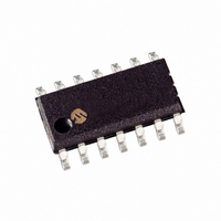
PIC16F630-I/SL Microchip Technology, PIC16F630-I/SL Datasheet - Page 43

PIC16F630-I/SL
Manufacturer Part Number
PIC16F630-I/SL
Description
IC MCU FLASH 1KX14 EEPROM 14SOIC
Manufacturer
Microchip Technology
Series
PIC® 16Fr
Datasheets
1.PIC16F616T-ISL.pdf
(8 pages)
2.PIC12F629T-ISN.pdf
(24 pages)
3.PIC16F630-ISL.pdf
(132 pages)
4.PIC16F630-ISL.pdf
(2 pages)
5.PIC16F630-ISL.pdf
(10 pages)
6.PIC16F676-EP.pdf
(132 pages)
7.PIC16F676-ISL.pdf
(130 pages)
Specifications of PIC16F630-I/SL
Program Memory Type
FLASH
Program Memory Size
1.75KB (1K x 14)
Package / Case
14-SOIC (3.9mm Width), 14-SOL
Core Processor
PIC
Core Size
8-Bit
Speed
20MHz
Peripherals
Brown-out Detect/Reset, POR, WDT
Number Of I /o
12
Eeprom Size
128 x 8
Ram Size
64 x 8
Voltage - Supply (vcc/vdd)
2 V ~ 5.5 V
Oscillator Type
Internal
Operating Temperature
-40°C ~ 85°C
Processor Series
PIC16F
Core
PIC
Data Bus Width
8 bit
Data Ram Size
64 B
Interface Type
RS- 232/USB
Maximum Clock Frequency
20 MHz
Number Of Programmable I/os
12
Number Of Timers
2
Operating Supply Voltage
2 V to 5.5 V
Maximum Operating Temperature
+ 85 C
Mounting Style
SMD/SMT
3rd Party Development Tools
52715-96, 52716-328, 52717-734
Development Tools By Supplier
PG164130, DV164035, DV244005, DV164005, PG164120, ICE2000, DM163014, DM164120-4
Minimum Operating Temperature
- 40 C
Package
14SOIC N
Device Core
PIC
Family Name
PIC16
Maximum Speed
20 MHz
Lead Free Status / RoHS Status
Lead free / RoHS Compliant
Data Converters
-
Connectivity
-
Lead Free Status / Rohs Status
Lead free / RoHS Compliant
Available stocks
Company
Part Number
Manufacturer
Quantity
Price
Company:
Part Number:
PIC16F630-I/SL
Manufacturer:
TriQuint
Quantity:
1 200
Company:
Part Number:
PIC16F630-I/SL
Manufacturer:
MICROCHI
Quantity:
1 743
Part Number:
PIC16F630-I/SL
Manufacturer:
MICROCHIP/微芯
Quantity:
20 000
6.5
The comparator module also allows the selection of an
internally generated voltage reference for one of the
comparator inputs. The internal reference signal is
used for four of the eight Comparator modes. The
VRCON register, Register 6-2, controls the voltage
reference module shown in Figure 6-5.
6.5.1
The voltage reference can output 32 distinct voltage
levels, 16 in a high range and 16 in a low range.
FIGURE 6-5:
6.6
Response time is the minimum time, after selecting a
new reference voltage or input source, before the
comparator output is ensured to have a valid level. If
the internal reference is changed, the maximum delay
of the internal voltage reference must be considered
when using the comparator outputs. Otherwise, the
maximum delay of the comparators should be used
(Table 12-7).
6.7
Both the comparator and voltage reference, if enabled
before entering Sleep mode, remain active during
Sleep. This results in higher Sleep currents than shown
in the power-down specifications. The additional cur-
rent consumed by the comparator and the voltage ref-
erence is shown separately in the specifications. To
minimize power consumption while in Sleep mode, turn
off the comparator, CM2:CM0 = 111, and voltage refer-
ence, VRCON<7> = 0.
2010 Microchip Technology Inc.
V
DD
Comparator
Comparator Reference
Comparator Response Time
Operation During Sleep
CV
CONFIGURING THE VOLTAGE
REFERENCE
REF
VREN
Input
to
COMPARATOR VOLTAGE REFERENCE BLOCK DIAGRAM
VR3:VR0
16-1 Analog
8R
MUX
R
R
16 Stages
The following equations determine the output voltages:
VRR = 1 (low range): CV
VRR = 0 (high range): CV
V
6.5.2
The full range of V
the construction of the module. The transistors on the
top and bottom of the resistor ladder network
(Figure 6-5) keep CV
V
fore, the CV
V
Voltage Reference can be found in Section 12.0
“Electrical Specifications”.
While the comparator is enabled during Sleep, an inter-
rupt will wake-up the device. If the device wakes up
from Sleep, the contents of the CMCON and VRCON
registers are not affected.
6.8
A device Reset forces the CMCON and VRCON
registers to their Reset states. This forces the
comparator module to be in the Comparator Reset
mode, CM2:CM0 = 000 and the voltage reference to its
off state. Thus, all potential inputs are analog inputs
with the comparator and voltage reference disabled to
consume the smallest current possible.
DD
DD
DD
. The tested absolute accuracy of the Comparator
. The Voltage Reference is V
/ 32)
R
Effects of a Reset
VOLTAGE REFERENCE
ACCURACY/ERROR
REF
PIC16F630/676
R
output changes with fluctuations in
SS
to V
REF
REF
REF
DD
= (VR3:VR0 / 24) x V
from approaching V
cannot be realized due to
= (V
8R
DD
DD
derived and there-
/ 4) + (VR3:VR0 x
DS40039F-page 43
VRR
DD
SS
or


