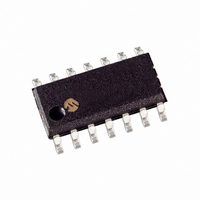
PIC16F630-I/SL Microchip Technology, PIC16F630-I/SL Datasheet - Page 50

PIC16F630-I/SL
Manufacturer Part Number
PIC16F630-I/SL
Description
IC MCU FLASH 1KX14 EEPROM 14SOIC
Manufacturer
Microchip Technology
Series
PIC® 16Fr
Datasheets
1.PIC16F616T-ISL.pdf
(8 pages)
2.PIC12F629T-ISN.pdf
(24 pages)
3.PIC16F630-ISL.pdf
(132 pages)
4.PIC16F630-ISL.pdf
(2 pages)
5.PIC16F630-ISL.pdf
(10 pages)
6.PIC16F676-EP.pdf
(132 pages)
7.PIC16F676-ISL.pdf
(130 pages)
Specifications of PIC16F630-I/SL
Program Memory Type
FLASH
Program Memory Size
1.75KB (1K x 14)
Package / Case
14-SOIC (3.9mm Width), 14-SOL
Core Processor
PIC
Core Size
8-Bit
Speed
20MHz
Peripherals
Brown-out Detect/Reset, POR, WDT
Number Of I /o
12
Eeprom Size
128 x 8
Ram Size
64 x 8
Voltage - Supply (vcc/vdd)
2 V ~ 5.5 V
Oscillator Type
Internal
Operating Temperature
-40°C ~ 85°C
Processor Series
PIC16F
Core
PIC
Data Bus Width
8 bit
Data Ram Size
64 B
Interface Type
RS- 232/USB
Maximum Clock Frequency
20 MHz
Number Of Programmable I/os
12
Number Of Timers
2
Operating Supply Voltage
2 V to 5.5 V
Maximum Operating Temperature
+ 85 C
Mounting Style
SMD/SMT
3rd Party Development Tools
52715-96, 52716-328, 52717-734
Development Tools By Supplier
PG164130, DV164035, DV244005, DV164005, PG164120, ICE2000, DM163014, DM164120-4
Minimum Operating Temperature
- 40 C
Package
14SOIC N
Device Core
PIC
Family Name
PIC16
Maximum Speed
20 MHz
Lead Free Status / RoHS Status
Lead free / RoHS Compliant
Data Converters
-
Connectivity
-
Lead Free Status / Rohs Status
Lead free / RoHS Compliant
Available stocks
Company
Part Number
Manufacturer
Quantity
Price
Company:
Part Number:
PIC16F630-I/SL
Manufacturer:
TriQuint
Quantity:
1 200
Company:
Part Number:
PIC16F630-I/SL
Manufacturer:
MICROCHI
Quantity:
1 743
Part Number:
PIC16F630-I/SL
Manufacturer:
MICROCHIP/微芯
Quantity:
20 000
PIC16F630/676
7.3
The A/D converter module can operate during Sleep.
This requires the A/D clock source to be set to the
internal oscillator. When the RC clock source is
selected, the A/D waits one instruction before starting
the conversion. This allows the SLEEP instruction to be
executed, thus eliminating much of the switching noise
from the conversion. When the conversion is complete,
the GO/DONE bit is cleared, and the result is loaded
into the ADRESH:ADRESL registers. If the A/D
interrupt is enabled, the device awakens from Sleep. If
the A/D interrupt is not enabled, the A/D module is
turned off, although the ADON bit remains set.
TABLE 7-2:
DS40039F-page 50
Address
05h
07h
0Bh, 8Bh INTCON
0Ch
1Eh
1Fh
85h
87h
8Ch
91h
9Eh
9Fh
Legend: x = unknown, u = unchanged, - = unimplemented read as ‘0’. Shaded cells are not used for A/D converter module.
A/D Operation During Sleep
PORTA
PORTC
PIR1
ADRESH Most Significant 8 bits of the Left Shifted A/D result or 2 bits of the Right Shifted Result
ADCON0
TRISA
TRISC
PIE1
ANSEL
ADRESL Least Significant 2 bits of the Left Shifted A/D Result or 8 bits of the Right Shifted Result
ADCON1
Name
SUMMARY OF A/D REGISTERS
ADFM
ANS7
EEIE
Bit 7
EEIF
GIE
—
—
—
—
—
ADCS2
VCFG
ANS6
PEIE
ADIF
ADIE
Bit 6
—
—
—
—
PORTC5 PORTC4 PORTC3 PORTC2 PORTC1 PORTC0 --xx xxxx --uu uuuu
PORTA5 PORTA4 PORTA3 PORTA2 PORTA1 PORTA0 --xx xxxx --uu uuuu
TRISA5
TRISC5
ADCS1
ANS5
Bit 5
T0IE
—
—
—
TRISA4
TRISC4
ADCS0
CHS2
ANS4
INTE
Bit 4
—
—
TRISA3
TRISC3
CHS1
ANS3
CMIF
CMIE
RAIE
Bit 3
—
When the A/D clock source is something other than
RC, a SLEEP instruction causes the present conversion
to be aborted, and the A/D module is turned off. The
ADON bit remains set.
7.4
A device Reset forces all registers to their Reset state.
Thus, the A/D module is turned off and any pending
conversion
registers are unchanged.
TRISC2
TRISA2
CHS0
ANS2
Bit 2
T0IF
—
—
—
Effects of Reset
is
TRISC1
TRISA1
ANS1
Bit 1
INTF
GO
—
—
—
aborted.
2010 Microchip Technology Inc.
TMR1IF 00-- 0--0 00-- 0--0
TRISC0 --11 1111 --11 1111
TMR1IE 00-- 0--0 00-- 0--0
TRISA0 --11 1111 --11 1111
ADON
ANS0
Bit 0
RAIF
—
The
0000 0000 0000 000u
xxxx xxxx uuuu uuuu
00-0 0000 00-0 0000
1111 1111 1111 1111
xxxx xxxx uuuu uuuu
-000 ---- -000 ----
POR, BOD
Value on
ADRESH:ADRESL
Value on
all other
Resets


