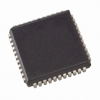
ATMEGA8535L-8JU Atmel, ATMEGA8535L-8JU Datasheet - Page 122

ATMEGA8535L-8JU
Manufacturer Part Number
ATMEGA8535L-8JU
Description
MCU AVR 8K ISP FLASH MEM 44-PLCC
Manufacturer
Atmel
Series
AVR® ATmegar
Specifications of ATMEGA8535L-8JU
Core Processor
AVR
Core Size
8-Bit
Speed
8MHz
Connectivity
I²C, SPI, UART/USART
Peripherals
Brown-out Detect/Reset, POR, PWM, WDT
Number Of I /o
32
Program Memory Size
8KB (4K x 16)
Program Memory Type
FLASH
Eeprom Size
512 x 8
Ram Size
512 x 8
Voltage - Supply (vcc/vdd)
2.7 V ~ 5.5 V
Data Converters
A/D 8x10b
Oscillator Type
Internal
Operating Temperature
-40°C ~ 85°C
Package / Case
44-PLCC
Processor Series
ATMEGA8x
Core
AVR8
Data Bus Width
8 bit
Data Ram Size
512 B
Interface Type
2-Wire, SPI, USART
Maximum Clock Frequency
8 MHz
Number Of Programmable I/os
32
Number Of Timers
3
Maximum Operating Temperature
+ 85 C
Mounting Style
SMD/SMT
3rd Party Development Tools
EWAVR, EWAVR-BL
Minimum Operating Temperature
- 40 C
On-chip Adc
10 bit, 8 Channel
Cpu Family
ATmega
Device Core
AVR
Device Core Size
8b
Frequency (max)
8MHz
Total Internal Ram Size
512Byte
# I/os (max)
32
Number Of Timers - General Purpose
3
Operating Supply Voltage (typ)
3.3/5V
Operating Supply Voltage (max)
5.5V
Operating Supply Voltage (min)
2.7V
Instruction Set Architecture
RISC
Operating Temp Range
-40C to 85C
Operating Temperature Classification
Industrial
Mounting
Surface Mount
Pin Count
44
Package Type
PLCC
For Use With
ATSTK600 - DEV KIT FOR AVR/AVR32770-1007 - ISP 4PORT ATMEL AVR MCU SPI/JTAGATAVRISP2 - PROGRAMMER AVR IN SYSTEMATSTK500 - PROGRAMMER AVR STARTER KIT
Lead Free Status / RoHS Status
Lead free / RoHS Compliant
Available stocks
Company
Part Number
Manufacturer
Quantity
Price
- Current page: 122 of 321
- Download datasheet (3Mb)
Modes of Operation
Normal Mode
Clear Timer on Compare
Match (CTC) Mode
122
ATmega8535(L)
A change of the COM21:0 bits state will take effect at the first Compare Match after the
bits are written. For non-PWM modes, the action can be forced to have an immediate
effect by using the FOC2 strobe bits.
The mode of operation (i.e., the behavior of the Timer/Counter and the Output Compare
pins) is defined by the combination of the Waveform Generation mode (WGM21:0) and
Compare Output mode (COM21:0) bits. The Compare Output mode bits do not affect
the counting sequence, while the Waveform Generation mode bits do. The COM21:0
bits control whether the PWM output generated should be inverted or not (inverted or
non-inverted PWM). For non-PWM modes the COM21:0 bits control whether the output
should be set, cleared, or toggled at a Compare Match (See “Compare Match Output
Unit” on page 121.).
For detailed timing information refer to “Timer/Counter Timing Diagrams” on page 126.
The simplest mode of operation is the Normal mode (WGM21:0 = 0). In this mode the
counting direction is always up (incrementing), and no counter clear is performed. The
counter simply overruns when it passes its maximum 8-bit value (TOP = 0xFF) and then
restarts from the bottom (0x00). In normal operation the Timer/Counter Overflow Flag
(TOV2) will be set in the same timer clock cycle as the TCNT2 becomes zero. The
TOV2 Flag in this case behaves like a ninth bit, except that it is only set, not cleared.
However, combined with the timer overflow interrupt that automatically clears the TOV2
Flag, the timer resolution can be increased by software. There are no special cases to
consider in the normal mode, a new counter value can be written anytime.
The output compare unit can be used to generate interrupts at some given time. Using
the output compare to generate waveforms in Normal mode is not recommended, since
this will occupy too much of the CPU time.
In Clear Timer on Compare or CTC mode (WGM21:0 = 2), the OCR2 Register is used to
manipulate the counter resolution. In CTC mode, the counter is cleared to zero when the
counter value (TCNT2) matches the OCR2. The OCR2 defines the top value for the
counter, hence also its resolution. This mode allows greater control of the Compare
Match output frequency. It also simplifies the operation of counting external events.
The timing diagram for the CTC mode is shown in Figure 57. The counter value
(TCNT2) increases until a Compare Match occurs between TCNT2 and OCR2, and then
counter (TCNT2) is cleared.
Figure 57. CTC Mode, Timing Diagram
TCNTn
OCn
(Toggle)
Period
1
2
3
4
OCn Interrupt Flag Set
(COMn1:0 = 1)
2502K–AVR–10/06
Related parts for ATMEGA8535L-8JU
Image
Part Number
Description
Manufacturer
Datasheet
Request
R

Part Number:
Description:
IC AVR MCU 2.4GHZ XCEIVER 64QFN
Manufacturer:
Atmel
Datasheet:

Part Number:
Description:
Manufacturer:
Atmel
Datasheet:

Part Number:
Description:
MCU ATMEGA644/AT86RF230 40-DIP
Manufacturer:
Atmel
Datasheet:

Part Number:
Description:
BUNDLE ATMEGA644P/AT86RF230 QFN
Manufacturer:
Atmel
Datasheet:

Part Number:
Description:
BUNDLE ATMEGA644P/AT86RF230 TQFP
Manufacturer:
Atmel
Datasheet:

Part Number:
Description:
MCU ATMEGA1281/AT86RF230 64-TQFP
Manufacturer:
Atmel
Datasheet:

Part Number:
Description:
MCU ATMEGA1280/AT86RF230 100TQFP
Manufacturer:
Atmel
Datasheet:

Part Number:
Description:
BUNDLE ATMEGA1280/AT86RF100-TQFP
Manufacturer:
Atmel
Datasheet:

Part Number:
Description:
BUNDLE ATMEGA2560V/AT86RF230-ZU
Manufacturer:
Atmel
Datasheet:

Part Number:
Description:
MCU ATMEGA2561/AT86RF230 64-TQFP
Manufacturer:
Atmel
Datasheet:

Part Number:
Description:
INTERVAL AND WIPE/WASH WIPER CONTROL IC WITH DELAY
Manufacturer:
ATMEL Corporation
Datasheet:

Part Number:
Description:
Low-Voltage Voice-Switched IC for Hands-Free Operation
Manufacturer:
ATMEL Corporation
Datasheet:

Part Number:
Description:
MONOLITHIC INTEGRATED FEATUREPHONE CIRCUIT
Manufacturer:
ATMEL Corporation
Datasheet:

Part Number:
Description:
AM-FM Receiver IC U4255BM-M
Manufacturer:
ATMEL Corporation
Datasheet:


