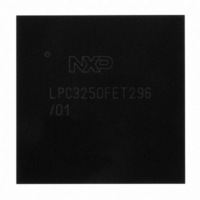
LPC3250FET296/01,5 NXP Semiconductors, LPC3250FET296/01,5 Datasheet - Page 32

LPC3250FET296/01,5
Manufacturer Part Number
LPC3250FET296/01,5
Description
IC ARM9 MCU 256K 296-TFBGA
Manufacturer
NXP Semiconductors
Series
LPC32x0r
Specifications of LPC3250FET296/01,5
Package / Case
296-TFBGA
Core Processor
ARM9
Core Size
16/32-Bit
Speed
266MHz
Connectivity
EBI/EMI, Ethernet, I²C, IrDA, Microwire, SPI, SSI, SSP, UART/USART, USB OTG
Peripherals
DMA, I²S, LCD, Motor Control PWM, PWM, WDT
Number Of I /o
51
Program Memory Type
ROMless
Ram Size
256K x 8
Voltage - Supply (vcc/vdd)
0.9 V ~ 3.6 V
Data Converters
A/D 3x10b
Oscillator Type
Internal
Operating Temperature
-40°C ~ 85°C
Processor Series
LPC32
Core
ARM926EJ-S
Data Bus Width
32 bit
Data Ram Size
256 KB
Interface Type
EMC
Maximum Clock Frequency
266 MHz
Number Of Timers
6
Operating Supply Voltage
1.31 V to 1.39 V
Maximum Operating Temperature
+ 85 C
Mounting Style
SMD/SMT
3rd Party Development Tools
MDK-ARM, RL-ARM, ULINK2, DK-57TS-LPC3250, DK-57VTS-LPC3250, SOMDIMM-LPC3250
Development Tools By Supplier
OM11016, OM11021, OM11045
Minimum Operating Temperature
- 40 C
On-chip Adc
10 bit, 3 Channel
Lead Free Status / RoHS Status
Lead free / RoHS Compliant
Eeprom Size
-
Program Memory Size
-
Lead Free Status / Rohs Status
Lead free / RoHS Compliant
Other names
568-4962
935290766551
935290766551
Available stocks
Company
Part Number
Manufacturer
Quantity
Price
Company:
Part Number:
LPC3250FET296/01,5
Manufacturer:
TI
Quantity:
250
Company:
Part Number:
LPC3250FET296/01,5
Manufacturer:
NXP Semiconductors
Quantity:
10 000
Part Number:
LPC3250FET296/01,5
Manufacturer:
NXP/恩智浦
Quantity:
20 000
NXP Semiconductors
LPC3220_30_40_50_1
Preliminary data sheet
7.7.4.1 Clocking
7.7.4.2 Crystal oscillator
7.7.4.3 PLLs
7.7.4 Clocking and power control features
Clocking in the LPC3220/30/40/50 is designed to be versatile, so that system and
peripheral requirements may be met, while allowing optimization of power consumption.
Clocks to most functions may be turned off if not needed and some peripherals do this
automatically.
The LPC3220/30/40/50 supports three operational modes, two of which are specifically
designed to reduce power consumption. The modes are: Run mode, Direct run mode, and
Stop mode.These three operational modes give control over processing speed and power
consumption. In addition, clock rates to different functional blocks may be changed by
switching clock sources, changing PLL values, or altering clock divider configurations.
This allows a trade-off of power versus processing speed based on application
requirements.
The main oscillator is the basis for the clocks most chip functions use by default.
Optionally, many functions can be clocked instead by the output of a PLL (with a fixed
397x rate multiplication) which runs from the RTC oscillator. In this mode, the main
oscillator may be turned off unless the USB interface is enabled. If a SYSCLK frequency
other than 13 MHz is required in the application, or if the USB block is not used, the main
oscillator may be used with a frequency of between 1 MHz and 20 MHz.
The LPC3220/30/40/50 includes three PLLs: The 397x PLL allows boosting the RTC
frequency to 13.008896 MHz for use as the primary system clock. The USB PLL provides
the 48 MHz clock required by the USB block, and the HCLK PLL provides the basis for the
CPU clock, the AHB bus clock, and the main peripheral clock.
The 397x PLL multiplies the 32768 Hz RTC clock by 397 to obtain a 13.008896 MHz
clock. The 397x PLL is designed for low power operation and low jitter. This PLL requires
an external RC loop filter for proper operation.
The HCLK PLL accepts an input clock from either the main oscillator or the output of the
397x PLL. The USB PLL only accepts an input clock from the main oscillator.The USB
input clock runs through a divide-by-N pre-divider before entering the USB PLL.
The input to the HCLK and USB PLLs may initially be divided down by a pre-divider value
‘N’, which may have the values 1, 2, 3, or 4. This pre-divider can allow a greater number of
possibilities for the output frequency. Following the PLL input divider is the PLL multiplier.
This can multiply the pre-divider output by a value ‘M’, in the range of 1 through 256. The
resulting frequency must be in the range of 156 MHz to 320 MHz. The multiplier works by
dividing the output of a Current Controlled Oscillator (CCO) by the value of M, then using
a phase detector to compare the divided CCO output to the pre-divider output. The error
value is used to adjust the CCO frequency.
At the PLL output, there is a post-divider that can be used to bring the CCO frequency
down to the desired PLL output frequency. The post-divider value can divide the CCO
output by 1, 2, 4, 8, or 16. The post-divider can also be bypassed, allowing the PLL CCO
Rev. 01 — 6 February 2009
LPC3220/30/40/50
16/32-bit ARM microcontrollers
© NXP B.V. 2009. All rights reserved.
32 of 73


