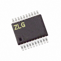
Z8F0411HH020SG Zilog, Z8F0411HH020SG Datasheet - Page 135

Z8F0411HH020SG
Manufacturer Part Number
Z8F0411HH020SG
Description
IC ENCORE MCU FLASH 4K 20SSOP
Manufacturer
Zilog
Series
Encore!® XP®r
Specifications of Z8F0411HH020SG
Core Processor
Z8
Core Size
8-Bit
Speed
20MHz
Connectivity
I²C, IrDA, UART/USART
Peripherals
Brown-out Detect/Reset, POR, PWM, WDT
Number Of I /o
11
Program Memory Size
4KB (4K x 8)
Program Memory Type
FLASH
Ram Size
1K x 8
Voltage - Supply (vcc/vdd)
2.7 V ~ 3.6 V
Oscillator Type
Internal
Operating Temperature
0°C ~ 70°C
Package / Case
20-SSOP
Controller Family/series
Z8
No. Of I/o's
11
Ram Memory Size
1KB
Cpu Speed
20MHz
No. Of Timers
2
Rohs Compliant
Yes
Processor Series
Z8F041xx
Core
eZ8
Data Bus Width
8 bit
Data Ram Size
1 KB
Interface Type
I2C, UART
Maximum Clock Frequency
20 MHz
Number Of Programmable I/os
11
Number Of Timers
2
Operating Supply Voltage
2.7 V to 3.6 V
Maximum Operating Temperature
+ 70 C
Mounting Style
SMD/SMT
Minimum Operating Temperature
0 C
For Use With
770-1002 - ISP 4PORT ZILOG Z8 ENCORE! MCU269-4643 - KIT DEV Z8 ENCORE XP 28-PIN269-4630 - DEV KIT FOR Z8 ENCORE 8K/4K269-4629 - KIT DEV Z8 ENCORE XP 28-PIN269-4628 - KIT DEV Z8 ENCORE XP 8-PIN
Lead Free Status / RoHS Status
Lead free / RoHS Compliant
Eeprom Size
-
Data Converters
-
Lead Free Status / Rohs Status
Details
Other names
269-4101
Z8F0411HH020SG
Z8F0411HH020SG
Available stocks
Company
Part Number
Manufacturer
Quantity
Price
Company:
Part Number:
Z8F0411HH020SG
Manufacturer:
Zilog
Quantity:
68
- Current page: 135 of 264
- Download datasheet (6Mb)
Table 64. SPI Control Register (SPICTL)
PS022517-0508
BITS
FIELD
RESET
R/W
ADDR
SPI Control Register
IRQE
7
The SPI Control Register configures the SPI for transmit and receive operations.
IRQE—Interrupt Request Enable
0 = SPI interrupts are disabled. No interrupt requests are sent to the Interrupt Controller.
1 = SPI interrupts are enabled. Interrupt requests are sent to the Interrupt Controller.
STR—Start an SPI Interrupt Request
0 = No effect.
1 = Setting this bit to 1 also sets the IRQ bit in the SPI Status Register to 1. Setting this
BIRQ—BRG Timer Interrupt Request
If the SPI is enabled, this bit has no effect. If the SPI is disabled:
0 = BRG timer function is disabled.
1 = BRG timer function and time-out interrupt are enabled.
PHASE—Phase Select
Sets the phase relationship of the data to the clock. For more information on operation of
the PHASE bit, see
CLKPOL—Clock Polarity
0 = SCK idles Low (0).
1 = SCK idle High (1).
WOR—Wire-OR (Open-Drain) Mode Enabled
0 = SPI signal pins not configured for open-drain.
1 = All four SPI signal pins (SCK, SS, MISO, MOSI) configured for open-drain function.
This setting is typically used for multi-master and/or multi-slave configurations.
MMEN—SPI MASTER Mode Enable
0 = SPI configured in SLAVE mode.
1 = SPI configured in MASTER mode.
SPIEN—SPI Enable
0 = SPI disabled.
1 = SPI enabled.
bit forces the SPI to send an interrupt request to the Interrupt Control. This bit can
be used by software for a function similar to transmit buffer empty in a UART.
Writing a 1 to the IRQ bit in the SPI Status Register clears this bit to 0.
STR
6
SPI Clock Phase and Polarity Control
BIRQ
5
PHASE
4
F61H
R/W
0
CLKPOL
3
Z8 Encore! XP
WOR
on page 116.
2
Product Specification
Serial Peripheral Interface
MMEN
1
®
F0822 Series
SPIEN
0
122
Related parts for Z8F0411HH020SG
Image
Part Number
Description
Manufacturer
Datasheet
Request
R

Part Number:
Description:
Communication Controllers, ZILOG INTELLIGENT PERIPHERAL CONTROLLER (ZIP)
Manufacturer:
Zilog, Inc.
Datasheet:

Part Number:
Description:
KIT DEV FOR Z8 ENCORE 16K TO 64K
Manufacturer:
Zilog
Datasheet:

Part Number:
Description:
KIT DEV Z8 ENCORE XP 28-PIN
Manufacturer:
Zilog
Datasheet:

Part Number:
Description:
DEV KIT FOR Z8 ENCORE 8K/4K
Manufacturer:
Zilog
Datasheet:

Part Number:
Description:
KIT DEV Z8 ENCORE XP 28-PIN
Manufacturer:
Zilog
Datasheet:

Part Number:
Description:
DEV KIT FOR Z8 ENCORE 4K TO 8K
Manufacturer:
Zilog
Datasheet:

Part Number:
Description:
CMOS Z8 microcontroller. ROM 16 Kbytes, RAM 256 bytes, speed 16 MHz, 32 lines I/O, 3.0V to 5.5V
Manufacturer:
Zilog, Inc.
Datasheet:

Part Number:
Description:
Low-cost microcontroller. 512 bytes ROM, 61 bytes RAM, 8 MHz
Manufacturer:
Zilog, Inc.
Datasheet:

Part Number:
Description:
Z8 4K OTP Microcontroller
Manufacturer:
Zilog, Inc.
Datasheet:

Part Number:
Description:
CMOS SUPER8 ROMLESS MCU
Manufacturer:
Zilog, Inc.
Datasheet:

Part Number:
Description:
SL1866 CMOSZ8 OTP Microcontroller
Manufacturer:
Zilog, Inc.
Datasheet:

Part Number:
Description:
SL1866 CMOSZ8 OTP Microcontroller
Manufacturer:
Zilog, Inc.
Datasheet:

Part Number:
Description:
OTP (KB) = 1, RAM = 125, Speed = 12, I/O = 14, 8-bit Timers = 2, Comm Interfaces Other Features = Por, LV Protect, Voltage = 4.5-5.5V
Manufacturer:
Zilog, Inc.
Datasheet:

Part Number:
Description:
Manufacturer:
Zilog, Inc.
Datasheet:


