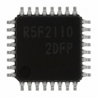
R5F21102DFP#U0 Renesas Electronics America, R5F21102DFP#U0 Datasheet - Page 63

R5F21102DFP#U0
Manufacturer Part Number
R5F21102DFP#U0
Description
IC R8C MCU FLASH 8K 32LQFP
Manufacturer
Renesas Electronics America
Series
M16C™ M16C/R8C/Tiny/10r
Datasheets
1.R5F211A2SPU0.pdf
(300 pages)
2.R5F21102FPU0.pdf
(30 pages)
3.R5F21102FPU0.pdf
(201 pages)
Specifications of R5F21102DFP#U0
Core Processor
R8C
Core Size
16-Bit
Speed
16MHz
Connectivity
SIO, UART/USART
Peripherals
LED, WDT
Number Of I /o
22
Program Memory Size
8KB (8K x 8)
Program Memory Type
FLASH
Ram Size
512 x 8
Voltage - Supply (vcc/vdd)
2.7 V ~ 5.5 V
Data Converters
A/D 8x10b
Oscillator Type
Internal
Operating Temperature
-40°C ~ 85°C
Package / Case
32-LQFP
For Use With
R0K521134S000BE - KIT EVAL STARTER FOR R8C/13R0E521134EPB00 - KIT EMULATOR PROBE FOR PC7501R0E521134CPE00 - EMULATOR COMPACT R8C/13
Lead Free Status / RoHS Status
Lead free / RoHS Compliant
Eeprom Size
-
Available stocks
Company
Part Number
Manufacturer
Quantity
Price
- Current page: 63 of 201
- Download datasheet (2Mb)
R8C/10 Group
Rev.1.20 Jan 27, 2006
REJ09B0019-0120
Table 10.6 Value of PC Saved to Stack when Address Match Interrupt Acknowledged
Table 10.7 Relationship Between Address Match Interrupt Factors and Associated Registers
Address match interrupt 0
Address match interrupt 1
10.4 Address Match Interrupt
• 16-bit operation code instruction
• Instruction shown below among 8-bit operation code instructions
• Instructions other than the above
Address match interrupt factors
An address match interrupt is generated immediately before executing the instruction at the address
indicated by the RMADi register (i=0, 1). Set the start address of any instruction in the RMADi register.
Use the AIER0 and AIER1 bits in the AIER register to enable or disable the interrupt. Note that the
address match interrupt is unaffected by the I flag and IPL.
The value of the PC that is saved to the stack when an address match interrupt is acknowledged varies
depending on the instruction at the address indicated by the RMAD i register (see the paragraph “register
saving” for the value of the PC). Not appropriate return address is pushed on the stack. There are two
ways to return from the address match interrupt as follows:
• Change the content of the stack and use a REIT instruction.
• Use an instruction such as POP to restore the stack as it was before an interrupt request was acknowl-
edged. And then use a jump instruction.
Table 10.6 lists the value of the PC that is saved to the stack when an address match interrupt is acknowl-
edged.
Figure 10.17 shows the AIER, and RMAD1 to RMAD0 registers.
ADD.B:S #IMM8,dest
OR.B:S
STNZ.B:S #IMM8,dest
CMP.B:S #IMM8,dest
JMPS
MOV.B:S #IMM,dest (However, dest = A0 or A1)
NOTES:
1. See the paragraph “saving registers” for the PC value saved.
Address indicated by RMADi register (i=0,1)
#IMM8,dest
#IMM8
page 51 of 180
SUB.B:S #IMM8,dest AND.B:S #IMM8,dest
MOV.B:S #IMM8,dest STZ.B:S #IMM8,dest
STZX.B:S #IMM81,#IMM82,dest
PUSHM
JSRS
Address match interrupt enable bit
AIER0
AIER1
src
#IMM8
POPM dest
RMAD0
RMAD1
Address match interrupt register
10.4 Address Match Interrupt
Address indicated by
RMADi register + 2
Address indicated by
RMADi register + 1
PC value saved
(1)
Related parts for R5F21102DFP#U0
Image
Part Number
Description
Manufacturer
Datasheet
Request
R

Part Number:
Description:
KIT STARTER FOR M16C/29
Manufacturer:
Renesas Electronics America
Datasheet:

Part Number:
Description:
KIT STARTER FOR R8C/2D
Manufacturer:
Renesas Electronics America
Datasheet:

Part Number:
Description:
R0K33062P STARTER KIT
Manufacturer:
Renesas Electronics America
Datasheet:

Part Number:
Description:
KIT STARTER FOR R8C/23 E8A
Manufacturer:
Renesas Electronics America
Datasheet:

Part Number:
Description:
KIT STARTER FOR R8C/25
Manufacturer:
Renesas Electronics America
Datasheet:

Part Number:
Description:
KIT STARTER H8S2456 SHARPE DSPLY
Manufacturer:
Renesas Electronics America
Datasheet:

Part Number:
Description:
KIT STARTER FOR R8C38C
Manufacturer:
Renesas Electronics America
Datasheet:

Part Number:
Description:
KIT STARTER FOR R8C35C
Manufacturer:
Renesas Electronics America
Datasheet:

Part Number:
Description:
KIT STARTER FOR R8CL3AC+LCD APPS
Manufacturer:
Renesas Electronics America
Datasheet:

Part Number:
Description:
KIT STARTER FOR RX610
Manufacturer:
Renesas Electronics America
Datasheet:

Part Number:
Description:
KIT STARTER FOR R32C/118
Manufacturer:
Renesas Electronics America
Datasheet:

Part Number:
Description:
KIT DEV RSK-R8C/26-29
Manufacturer:
Renesas Electronics America
Datasheet:

Part Number:
Description:
KIT STARTER FOR SH7124
Manufacturer:
Renesas Electronics America
Datasheet:

Part Number:
Description:
KIT STARTER FOR H8SX/1622
Manufacturer:
Renesas Electronics America
Datasheet:

Part Number:
Description:
KIT DEV FOR SH7203
Manufacturer:
Renesas Electronics America
Datasheet:


