R5F21102DFP#U0 Renesas Electronics America, R5F21102DFP#U0 Datasheet - Page 98
R5F21102DFP#U0
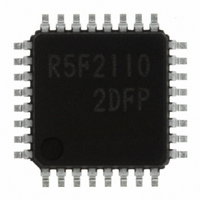
Manufacturer Part Number
R5F21102DFP#U0
Description
IC R8C MCU FLASH 8K 32LQFP
Manufacturer
Renesas Electronics America
Series
M16C™ M16C/R8C/Tiny/10r
Datasheets
1.R5F211A2SPU0.pdf
(300 pages)
2.R5F21102FPU0.pdf
(30 pages)
3.R5F21102FPU0.pdf
(201 pages)
Specifications of R5F21102DFP#U0
Core Processor
R8C
Core Size
16-Bit
Speed
16MHz
Connectivity
SIO, UART/USART
Peripherals
LED, WDT
Number Of I /o
22
Program Memory Size
8KB (8K x 8)
Program Memory Type
FLASH
Ram Size
512 x 8
Voltage - Supply (vcc/vdd)
2.7 V ~ 5.5 V
Data Converters
A/D 8x10b
Oscillator Type
Internal
Operating Temperature
-40°C ~ 85°C
Package / Case
32-LQFP
For Use With
R0K521134S000BE - KIT EVAL STARTER FOR R8C/13R0E521134EPB00 - KIT EMULATOR PROBE FOR PC7501R0E521134CPE00 - EMULATOR COMPACT R8C/13
Lead Free Status / RoHS Status
Lead free / RoHS Compliant
Eeprom Size
-
Available stocks
Company
Part Number
Manufacturer
Quantity
Price


R8C/10 Group
Rev.1.20 Jan 27, 2006
REJ09B0019-0120
Figure 12.28 Timer C Block Diagram
Table 12.13 Timer C Specifications
NOTES:
12.4 Timer C
1. TC register and TM0 register must be read in 16-bit units.
Count source
Count operation
Count start condition
Count stop condition
Interrupt request
generation timing
______
INT3/TC
Counter value reset timing
Read from timer
Write to timer
Select function
Timer C is a 16-bit free-running timer. Figure 12.28 shows a block diagram of Timer C. The Timer C uses
an edge input to TC
interrupt request. The TC
from occurring. Table 12.13 shows Timer C specifications. Figure 12.29 shows TC, TM0, TCC0, and
TCC1 registers. Figure 12.30 shows an operation example of Timer C.
INT3/TC
TCC11 to TCC10
TCC11 to TCC10
IN
Item
IN
Other than 00
f
32
f
pin function
f
8
1
(1)
=01
=10
=11
=00
TCC02 to TCC01
2
2
2
page 86 of 180
2
2
Sampling
clock
IN
f
pin or the f
Digital
f
f
32
1
8
filter
f
RING128
f
• Count up
• Transfer value in TC register to TM0 register at active edge of measurement pulse
• Value in TC register is set to “0000
TCC00 bit in TCC0 register is set to “1” (capture enabled)
TCC00 bit in TCC0 register is set to “0” (capture disabled)
• When active edge of measurement pulse is input [INT3 interrupt]
• When Time C underflows [Timer C interrupt]
Programmable I/O or measurement pulse input
When TCC00 bit in TCC0 register is set to “0” (capture disabled)
• Counter value can be read out by reading TC register.
• Counter value at measurement pulse active edge input can be read out by reading TM0
Write to TC register and TM0 register is disabled
• INT3/TC
• Digital filter function
• Trigger select function
1
IN
register.
Measurement pulse active edge is selected by TCC03 to TCC04 bits
Digital filter sampling frequency is selected by TCC11 to TCC10 bits
TC
, f
_____
=00
=01
=10
input has a digital filter and this prevents an error caused by noise or so on
8
IN
, f
2
2
2
32
input or f
TCC07=0
RING128
TCC07=1
IN
switching function
RING128
Edge detection
clock as trigger to latch the timer count value and generates an
TCC01, TCC02, TCC07: Bits in TCC0 register
TCC10, TCC11: Bits in TCC1 register
Upper 8 bits
Upper 8 bits
is selected by TCC07 bit.
TM0 register
TC register
Counter
Specification
16
Lower 8 bits
Lower 8 bits
” when a counting stops
Data bus
_____
Transfer signal
Timer C interrupt
INT3 interrupt
12.4 Timer (Timer C)
Related parts for R5F21102DFP#U0
Image
Part Number
Description
Manufacturer
Datasheet
Request
R

Part Number:
Description:
KIT STARTER FOR M16C/29
Manufacturer:
Renesas Electronics America
Datasheet:

Part Number:
Description:
KIT STARTER FOR R8C/2D
Manufacturer:
Renesas Electronics America
Datasheet:

Part Number:
Description:
R0K33062P STARTER KIT
Manufacturer:
Renesas Electronics America
Datasheet:

Part Number:
Description:
KIT STARTER FOR R8C/23 E8A
Manufacturer:
Renesas Electronics America
Datasheet:

Part Number:
Description:
KIT STARTER FOR R8C/25
Manufacturer:
Renesas Electronics America
Datasheet:

Part Number:
Description:
KIT STARTER H8S2456 SHARPE DSPLY
Manufacturer:
Renesas Electronics America
Datasheet:

Part Number:
Description:
KIT STARTER FOR R8C38C
Manufacturer:
Renesas Electronics America
Datasheet:

Part Number:
Description:
KIT STARTER FOR R8C35C
Manufacturer:
Renesas Electronics America
Datasheet:

Part Number:
Description:
KIT STARTER FOR R8CL3AC+LCD APPS
Manufacturer:
Renesas Electronics America
Datasheet:
Part Number:
Description:
KIT STARTER FOR RX610
Manufacturer:
Renesas Electronics America
Datasheet:

Part Number:
Description:
KIT STARTER FOR R32C/118
Manufacturer:
Renesas Electronics America
Datasheet:

Part Number:
Description:
KIT DEV RSK-R8C/26-29
Manufacturer:
Renesas Electronics America
Datasheet:

Part Number:
Description:
KIT STARTER FOR SH7124
Manufacturer:
Renesas Electronics America
Datasheet:

Part Number:
Description:
KIT STARTER FOR H8SX/1622
Manufacturer:
Renesas Electronics America
Datasheet:

Part Number:
Description:
KIT DEV FOR SH7203
Manufacturer:
Renesas Electronics America
Datasheet: