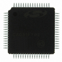
C8051F702-GQ Silicon Laboratories Inc, C8051F702-GQ Datasheet - Page 79

C8051F702-GQ
Manufacturer Part Number
C8051F702-GQ
Description
IC 8051 MCU 16K FLASH 64-TQFP
Manufacturer
Silicon Laboratories Inc
Series
C8051F70xr
Specifications of C8051F702-GQ
Program Memory Type
FLASH
Program Memory Size
16KB (16K x 8)
Package / Case
64-TQFP, 64-VQFP
Core Processor
8051
Core Size
8-Bit
Speed
25MHz
Connectivity
EBI/EMI, SMBus (2-Wire/I²C), SPI, UART/USART
Peripherals
Cap Sense, POR, PWM, Temp Sensor, WDT
Number Of I /o
54
Ram Size
512 x 8
Voltage - Supply (vcc/vdd)
1.8 V ~ 3.6 V
Data Converters
A/D 16x10b
Oscillator Type
Internal
Operating Temperature
-40°C ~ 85°C
Processor Series
C8051F7x
Core
8051
Data Bus Width
8 bit
Data Ram Size
512 B
Interface Type
I2C, SPI, UART
Maximum Clock Frequency
25 MHz
Number Of Programmable I/os
54
Number Of Timers
4 x 16 bit
Operating Supply Voltage
1.8 V to 3.3 V
Maximum Operating Temperature
+ 85 C
Mounting Style
SMD/SMT
3rd Party Development Tools
PK51, CA51, A51, ULINK2
Development Tools By Supplier
C8051F700DK
Minimum Operating Temperature
- 40 C
On-chip Adc
10 bit, 16 Channel
Lead Free Status / RoHS Status
Lead free / RoHS Compliant
For Use With
336-1635 - DEV KIT FOR C8051F700
Eeprom Size
-
Lead Free Status / Rohs Status
Lead free / RoHS Compliant
Other names
336-1608
Available stocks
Company
Part Number
Manufacturer
Quantity
Price
Company:
Part Number:
C8051F702-GQ
Manufacturer:
Silicon Laboratories Inc
Quantity:
10 000
Company:
Part Number:
C8051F702-GQR
Manufacturer:
Silicon Laboratories Inc
Quantity:
10 000
- Current page: 79 of 306
- Download datasheet (2Mb)
SFR Definition 14.3. CPT0MX: Comparator0 MUX Selection
SFR Address = 0x9F; SFR Page = 0
Note: On 32 and 24-pin devices, P2.0 can be used as the negative comparator input, for detecting low-level signals
Name
Reset
Bit
6:4 CMX0N[2:0] Comparator0 Negative Input MUX Selection.
2:0
Type
7
3
Bit
CMX0P[2:0] Comparator0 Positive Input MUX Selection.
near the GND or VDD supply rails. The P1.6 setting for the positive input should be used in conjunction with
the selection of P2.0 as the negative input. P1.6 should be configured for push-pull mode and driven to the
desired supply rail. Although P1.6 is not connected to a device pin in these packages, it is still a valid signal
internally.
Unused
Unused
Name
R
7
0
Read = 0b; Write = don’t care.
Read = 0b; Write = don’t care.
100-111
100-111
000
001
010
011
000
001
010
011
6
0
64-Pin Devices
64-Pin Devices
CMX0N[2:0]
selected.
selected.
No input
No input
R/W
P1.1
P1.3
P1.5
P1.7
P1.0
P1.2
P1.4
P1.6
5
0
Rev. 1.0
4
0
48-Pin Devices
48-Pin Devices
selected.
selected.
No input
No input
P1.1
P1.3
P1.0
P1.2
—
—
—
—
Function
R
3
0
(P1.6—see note) (P1.6—see note)
32-Pin Devices
32-Pin Devices
P2.0 (see note)
selected.
selected.
C8051F70x/71x
No input
No input
2
0
—
—
—
—
—
—
CMX0P[2:0]
R/W
1
0
24-Pin Devices
24-Pin Devices
P2.0 (see note)
selected.
selected.
No input
No input
—
—
—
—
—
—
0
0
79
Related parts for C8051F702-GQ
Image
Part Number
Description
Manufacturer
Datasheet
Request
R
Part Number:
Description:
SMD/C°/SINGLE-ENDED OUTPUT SILICON OSCILLATOR
Manufacturer:
Silicon Laboratories Inc
Part Number:
Description:
Manufacturer:
Silicon Laboratories Inc
Datasheet:
Part Number:
Description:
N/A N/A/SI4010 AES KEYFOB DEMO WITH LCD RX
Manufacturer:
Silicon Laboratories Inc
Datasheet:
Part Number:
Description:
N/A N/A/SI4010 SIMPLIFIED KEY FOB DEMO WITH LED RX
Manufacturer:
Silicon Laboratories Inc
Datasheet:
Part Number:
Description:
N/A/-40 TO 85 OC/EZLINK MODULE; F930/4432 HIGH BAND (REV E/B1)
Manufacturer:
Silicon Laboratories Inc
Part Number:
Description:
EZLink Module; F930/4432 Low Band (rev e/B1)
Manufacturer:
Silicon Laboratories Inc
Part Number:
Description:
I°/4460 10 DBM RADIO TEST CARD 434 MHZ
Manufacturer:
Silicon Laboratories Inc
Part Number:
Description:
I°/4461 14 DBM RADIO TEST CARD 868 MHZ
Manufacturer:
Silicon Laboratories Inc
Part Number:
Description:
I°/4463 20 DBM RFSWITCH RADIO TEST CARD 460 MHZ
Manufacturer:
Silicon Laboratories Inc
Part Number:
Description:
I°/4463 20 DBM RADIO TEST CARD 868 MHZ
Manufacturer:
Silicon Laboratories Inc
Part Number:
Description:
I°/4463 27 DBM RADIO TEST CARD 868 MHZ
Manufacturer:
Silicon Laboratories Inc
Part Number:
Description:
I°/4463 SKYWORKS 30 DBM RADIO TEST CARD 915 MHZ
Manufacturer:
Silicon Laboratories Inc
Part Number:
Description:
N/A N/A/-40 TO 85 OC/4463 RFMD 30 DBM RADIO TEST CARD 915 MHZ
Manufacturer:
Silicon Laboratories Inc
Part Number:
Description:
I°/4463 20 DBM RADIO TEST CARD 169 MHZ
Manufacturer:
Silicon Laboratories Inc


