MC9S12E64CFUE Freescale Semiconductor, MC9S12E64CFUE Datasheet - Page 448
MC9S12E64CFUE
Manufacturer Part Number
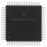
MC9S12E64CFUE
Description
IC MCU 64K FLASH 25MHZ 80-QFP
Manufacturer
Freescale Semiconductor
Series
HCS12r
Specifications of MC9S12E64CFUE
Core Processor
HCS12
Core Size
16-Bit
Speed
25MHz
Connectivity
EBI/EMI, I²C, SCI, SPI
Peripherals
POR, PWM, WDT
Number Of I /o
60
Program Memory Size
64KB (64K x 8)
Program Memory Type
FLASH
Ram Size
4K x 8
Voltage - Supply (vcc/vdd)
2.35 V ~ 2.75 V
Data Converters
A/D 16x10b; D/A 2x8b
Oscillator Type
Internal
Operating Temperature
-40°C ~ 85°C
Package / Case
80-QFP
Package
80PQFP
Family Name
HCS12
Maximum Speed
25 MHz
Operating Supply Voltage
2.5|3.3|5 V
Data Bus Width
16 Bit
Number Of Programmable I/os
60
Interface Type
SCI/SPI
On-chip Adc
16-chx10-bit
On-chip Dac
2-chx8-bit
Number Of Timers
12
Processor Series
S12E
Core
HCS12
Data Ram Size
4 KB
Maximum Clock Frequency
25 MHz
Maximum Operating Temperature
+ 85 C
Mounting Style
SMD/SMT
3rd Party Development Tools
EWHCS12
Minimum Operating Temperature
- 40 C
Controller Family/series
HCS12/S12X
No. Of I/o's
58
Ram Memory Size
4KB
Cpu Speed
25MHz
No. Of Timers
4
Embedded Interface Type
I2C, SCI, SPI
Rohs Compliant
Yes
For Use With
M68EVB912E128 - BOARD EVAL FOR MC9S12E128/64
Lead Free Status / RoHS Status
Lead free / RoHS Compliant
Eeprom Size
-
Lead Free Status / Rohs Status
Lead free / RoHS Compliant
Available stocks
Company
Part Number
Manufacturer
Quantity
Price
Company:

Part Number:
MC9S12E64CFUE
Manufacturer:
Freescale Semiconductor
Quantity:
10 000
Part Number:
MC9S12E64CFUE
Manufacturer:
FREESCALE
Quantity:
20 000
Company:
Part Number:
MC9S12E64CFUER
Manufacturer:
Freescale Semiconductor
Quantity:
10 000


Chapter 15 Background Debug Module (BDMV4)
15.1.2
BDM is available in all operating modes but must be enabled before firmware commands are executed.
Some system peripherals may have a control bit which allows suspending the peripheral function during
background debug mode.
15.1.2.1
All of these operations refer to the part in run mode. The BDM does not provide controls to conserve power
during run mode.
15.1.2.2
If the part is in secure mode, the operation of the BDM is reduced to a small subset of its regular run mode
operation. Secure operation prevents access to FLASH or EEPROM other than allowing erasure.
15.2
A single-wire interface pin is used to communicate with the BDM system. Two additional pins are used
for instruction tagging. These pins are part of the multiplexed external bus interface (MEBI) sub-block and
all interfacing between the MEBI and BDM is done within the core interface boundary. Functional
descriptions of the pins are provided below for completeness.
448
•
•
•
•
•
•
•
•
•
•
•
Nine hardware commands using free cycles, if available, for minimal CPU intervention
Hardware commands not requiring active BDM
15 firmware commands execute from the standard BDM firmware lookup table
Instruction tagging capability
Software control of BDM operation during wait mode
Software selectable clocks
When secured, hardware commands are allowed to access the register space in special single-chip
mode, if the FLASH and EEPROM erase tests fail.
Normal operation
General operation of the BDM is available and operates the same in all normal modes.
Special single-chip mode
In special single-chip mode, background operation is enabled and active out of reset. This allows
programming a system with blank memory.
Special peripheral mode
Emulation modes
General operation of the BDM is available and operates the same as in normal modes.
External Signal Description
Modes of Operation
Regular Run Modes
Secure Mode Operation
BDM is enabled and active immediately out of reset. BDM can be disabled
by clearing the BDMACT bit in the BDM status (BDMSTS) register. The
BDM serial system should not be used in special peripheral mode.
MC9S12E128 Data Sheet, Rev. 1.07
Freescale Semiconductor
Related parts for MC9S12E64CFUE
Image
Part Number
Description
Manufacturer
Datasheet
Request
R

Part Number:
Description:
Manufacturer:
Freescale Semiconductor, Inc
Datasheet:
Part Number:
Description:
Manufacturer:
Freescale Semiconductor, Inc
Datasheet:
Part Number:
Description:
Manufacturer:
Freescale Semiconductor, Inc
Datasheet:
Part Number:
Description:
Manufacturer:
Freescale Semiconductor, Inc
Datasheet:
Part Number:
Description:
Manufacturer:
Freescale Semiconductor, Inc
Datasheet:
Part Number:
Description:
Manufacturer:
Freescale Semiconductor, Inc
Datasheet:
Part Number:
Description:
Manufacturer:
Freescale Semiconductor, Inc
Datasheet:
Part Number:
Description:
Manufacturer:
Freescale Semiconductor, Inc
Datasheet:
Part Number:
Description:
Manufacturer:
Freescale Semiconductor, Inc
Datasheet:
Part Number:
Description:
Manufacturer:
Freescale Semiconductor, Inc
Datasheet:
Part Number:
Description:
Manufacturer:
Freescale Semiconductor, Inc
Datasheet:
Part Number:
Description:
Manufacturer:
Freescale Semiconductor, Inc
Datasheet:
Part Number:
Description:
Manufacturer:
Freescale Semiconductor, Inc
Datasheet:
Part Number:
Description:
Manufacturer:
Freescale Semiconductor, Inc
Datasheet:
Part Number:
Description:
Manufacturer:
Freescale Semiconductor, Inc
Datasheet: