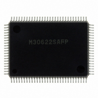
M30622SAFP#U5 Renesas Electronics America, M30622SAFP#U5 Datasheet - Page 323

M30622SAFP#U5
Manufacturer Part Number
M30622SAFP#U5
Description
IC M16C MPU ROMLESS 100QFP
Manufacturer
Renesas Electronics America
Series
M16C™ M16C/60r
Datasheets
1.QSK-62P_PLUS.pdf
(103 pages)
2.M30622SAFPU5.pdf
(277 pages)
3.M30622SAFPU5.pdf
(617 pages)
4.M30622SAFPU5.pdf
(308 pages)
Specifications of M30622SAFP#U5
Core Processor
M16C/60
Core Size
16-Bit
Speed
16MHz
Connectivity
SIO, UART/USART
Peripherals
DMA, PWM, WDT
Number Of I /o
50
Program Memory Type
ROMless
Ram Size
3K x 8
Voltage - Supply (vcc/vdd)
4.2 V ~ 5.5 V
Data Converters
A/D 10x10b, D/A 2x8b
Oscillator Type
Internal
Operating Temperature
-20°C ~ 85°C
Package / Case
100-QFP
For Use With
867-1000 - KIT QUICK START RENESAS 62PM3062PT3-CPE-3 - EMULATOR COMPACT M16C/62P/30P
Lead Free Status / RoHS Status
Lead free / RoHS Compliant
Eeprom Size
-
Program Memory Size
-
Available stocks
Company
Part Number
Manufacturer
Quantity
Price
- QSK-62P_PLUS PDF datasheet
- M30622SAFPU5 PDF datasheet #2
- M30622SAFPU5 PDF datasheet #3
- M30622SAFPU5 PDF datasheet #4
- Current page: 323 of 617
- Download datasheet (9Mb)
Protect
2-4
Operation
2.1.2 Protect Operation
The following explains the protect operation. Figure 2.1.2 shows the set-up procedure.
(1) Setting “1” in the write-enable bit of system clock control registers 0 and 1 causes system
(2) The contents of system clock control register 0 and that of system clock control register 1 are changed.
(3) Setting “0” in the write-enable bit of system control registers 0 and 1 causes system clock
(4) To change the contents of processor mode register 0 and that of processor mode register 1,
(5) The write-enable bit of port 9 direction register and SI/Oi control register (i=3,4) goes to “0”
clock control register 0 and system clock control register 1 to be in write-enabled state.
control register 0 and system control register 1 to be in write-inhibited state.
follow the same steps as in dealing with system clock control registers.
when the next write instruction is executed after write-enabled state is readied. Make
changes in input/output and SI/Oi control register (i=3,4) immediately after the instruction that
sets “1” in the write-enable bit of port P9 direction register and SI/Oi control register
(i=3,4)(avoid causing an interrupt). Also take measures to prevent DMA transfer from being
executed.
SINGLE-CHIP 16-BIT CMOS MICROCOMPUTER
M16C / 62A Group
Mitsubishi microcomputers
Related parts for M30622SAFP#U5
Image
Part Number
Description
Manufacturer
Datasheet
Request
R

Part Number:
Description:
KIT STARTER FOR M16C/29
Manufacturer:
Renesas Electronics America
Datasheet:

Part Number:
Description:
KIT STARTER FOR R8C/2D
Manufacturer:
Renesas Electronics America
Datasheet:

Part Number:
Description:
R0K33062P STARTER KIT
Manufacturer:
Renesas Electronics America
Datasheet:

Part Number:
Description:
KIT STARTER FOR R8C/23 E8A
Manufacturer:
Renesas Electronics America
Datasheet:

Part Number:
Description:
KIT STARTER FOR R8C/25
Manufacturer:
Renesas Electronics America
Datasheet:

Part Number:
Description:
KIT STARTER H8S2456 SHARPE DSPLY
Manufacturer:
Renesas Electronics America
Datasheet:

Part Number:
Description:
KIT STARTER FOR R8C38C
Manufacturer:
Renesas Electronics America
Datasheet:

Part Number:
Description:
KIT STARTER FOR R8C35C
Manufacturer:
Renesas Electronics America
Datasheet:

Part Number:
Description:
KIT STARTER FOR R8CL3AC+LCD APPS
Manufacturer:
Renesas Electronics America
Datasheet:

Part Number:
Description:
KIT STARTER FOR RX610
Manufacturer:
Renesas Electronics America
Datasheet:

Part Number:
Description:
KIT STARTER FOR R32C/118
Manufacturer:
Renesas Electronics America
Datasheet:

Part Number:
Description:
KIT DEV RSK-R8C/26-29
Manufacturer:
Renesas Electronics America
Datasheet:

Part Number:
Description:
KIT STARTER FOR SH7124
Manufacturer:
Renesas Electronics America
Datasheet:

Part Number:
Description:
KIT STARTER FOR H8SX/1622
Manufacturer:
Renesas Electronics America
Datasheet:

Part Number:
Description:
KIT DEV FOR SH7203
Manufacturer:
Renesas Electronics America
Datasheet:


