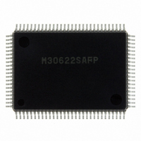
M30622SAFP#U5 Renesas Electronics America, M30622SAFP#U5 Datasheet - Page 373

M30622SAFP#U5
Manufacturer Part Number
M30622SAFP#U5
Description
IC M16C MPU ROMLESS 100QFP
Manufacturer
Renesas Electronics America
Series
M16C™ M16C/60r
Datasheets
1.QSK-62P_PLUS.pdf
(103 pages)
2.M30622SAFPU5.pdf
(277 pages)
3.M30622SAFPU5.pdf
(617 pages)
4.M30622SAFPU5.pdf
(308 pages)
Specifications of M30622SAFP#U5
Core Processor
M16C/60
Core Size
16-Bit
Speed
16MHz
Connectivity
SIO, UART/USART
Peripherals
DMA, PWM, WDT
Number Of I /o
50
Program Memory Type
ROMless
Ram Size
3K x 8
Voltage - Supply (vcc/vdd)
4.2 V ~ 5.5 V
Data Converters
A/D 10x10b, D/A 2x8b
Oscillator Type
Internal
Operating Temperature
-20°C ~ 85°C
Package / Case
100-QFP
For Use With
867-1000 - KIT QUICK START RENESAS 62PM3062PT3-CPE-3 - EMULATOR COMPACT M16C/62P/30P
Lead Free Status / RoHS Status
Lead free / RoHS Compliant
Eeprom Size
-
Program Memory Size
-
Available stocks
Company
Part Number
Manufacturer
Quantity
Price
- QSK-62P_PLUS PDF datasheet
- M30622SAFPU5 PDF datasheet #2
- M30622SAFPU5 PDF datasheet #3
- M30622SAFPU5 PDF datasheet #4
- Current page: 373 of 617
- Download datasheet (9Mb)
Clock-Synchronous Serial I/O
2-54
Figure 2.4.1. Memory map of serial I/O-related registers
Following are some examples in which various functions (a) through (g) are selected:
(6) Input to the serial I/O and the direction register
(7) Pins related to the serial I/O
(8) Registers related to the serial I/O
To input an external signal to the serial I/O, set the direction register of the relevant port to input.
• CTS
• RTS
• CLK
• RxD
• TxD
• CLKS
Figure 2.4.1 shows the memory map of serial I/O-related registers, and Figures 2.4.2 to 2.4.6 show
serial I/O-related registers.
• Transmission Operation WITH: CTS function, transmission at falling edge of transfer clock, LSB
• Transmission Operation WITH: CTS/RTS function disabled, transmission at falling edge of transfer
• Reception WITH: RTS function, reception at falling edge of transfer clock, LSB First, successive
_______
________
First, interrupt at instant transmission buffer is emptied; WITHOUT transfer clock output to multiple
pins function ........................................................................................................................... P2-60
clock, LSB First, interrupt at instant transmission is completed; WITH transfer clock output to mul-
tiple pins function (UART0 selection available) ...................................................................... P2-64
reception mode disabled; WITHOUT transfer clock output to multiple pins function ............. P2-68
0
0
0
0
0
, TxD
, RxD
, CTS
, RTS
, CLK
1
________
________
pin
1
1
1
1
1
, TxD
, CLK
, RxD
, CTS
, RTS
________
________
2
2
2
2
2
pins
_______
pins
pins
pins
pins
03A0
03A1
03A2
03A3
03A4
03A5
03A6
03A7
03A8
03A9
03AA
03AB
03AC
03AD
03AE
03AF
03B0
03B1
004F
0050
0051
0052
0053
0054
0378
0379
037A
037B
037C
037D
037E
037F
16
16
16
16
16
16
16
16
16
16
16
16
16
16
16
16
16
16
16
16
16
16
16
16
16
16
16
16
16
16
16
16
Output pin for transfer clock. Can be used as transfer clock output pin in
Input pins for the CTS function
Output pins for the RTS function
Input/output pins for the transfer clock
Input pins for data
Output pins for data (Since T
needs pull-up resistor.)
the transfer clock output to multiple pins function.
UART2 transmit interrupt control register (S2TIC)
UART2 receive interrupt control register (S2RIC)
UART0 transmit interrupt control register (S0TIC)
UART0 receive interrupt control register (S0RIC)
UART1 transmit interrupt control regster(S1TIC)
UART1 receive interrupt control register(S1RIC)
UART2 transmit/receive mode register (U2MR)
UART2 bit rate generator (U2BRG)
UART2 transmit buffer register (U2TB)
UART2 transmit/receive control register 0 (U2C0)
UART2 transmit/receive control register 1 (U2C1)
UART2 receive buffer register (U2RB)
UART0 transmit/receive mode register (U0MR)
UART0 bit rate generator (U0BRG)
UART0 transmit buffer register (U0TB)
UART0 transmit/receive control register 0 (U0C0)
UART0 transmit/receive control register 1 (U0C1)
UART0 receive buffer register (U0RB)
UART1 transmit/receive mode register (U1MR)
UART1 bit rate generator (U1BRG)
UART1 transmit buffer register (U1TB)
UART1 transmit/receive control register 0 (U1C0)
UART1 transmit/receive control register 1 (U1C1)
UART1 receive buffer register (U1RB)
UART transmit/receive control register 2 (UCON)
_______ _______
_______
_______
_______
X
D
2
pin is N-channel open drain, this pin
SINGLE-CHIP 16-BIT CMOS MICROCOMPUTER
M16C / 62A Group
Mitsubishi microcomputers
Related parts for M30622SAFP#U5
Image
Part Number
Description
Manufacturer
Datasheet
Request
R

Part Number:
Description:
KIT STARTER FOR M16C/29
Manufacturer:
Renesas Electronics America
Datasheet:

Part Number:
Description:
KIT STARTER FOR R8C/2D
Manufacturer:
Renesas Electronics America
Datasheet:

Part Number:
Description:
R0K33062P STARTER KIT
Manufacturer:
Renesas Electronics America
Datasheet:

Part Number:
Description:
KIT STARTER FOR R8C/23 E8A
Manufacturer:
Renesas Electronics America
Datasheet:

Part Number:
Description:
KIT STARTER FOR R8C/25
Manufacturer:
Renesas Electronics America
Datasheet:

Part Number:
Description:
KIT STARTER H8S2456 SHARPE DSPLY
Manufacturer:
Renesas Electronics America
Datasheet:

Part Number:
Description:
KIT STARTER FOR R8C38C
Manufacturer:
Renesas Electronics America
Datasheet:

Part Number:
Description:
KIT STARTER FOR R8C35C
Manufacturer:
Renesas Electronics America
Datasheet:

Part Number:
Description:
KIT STARTER FOR R8CL3AC+LCD APPS
Manufacturer:
Renesas Electronics America
Datasheet:

Part Number:
Description:
KIT STARTER FOR RX610
Manufacturer:
Renesas Electronics America
Datasheet:

Part Number:
Description:
KIT STARTER FOR R32C/118
Manufacturer:
Renesas Electronics America
Datasheet:

Part Number:
Description:
KIT DEV RSK-R8C/26-29
Manufacturer:
Renesas Electronics America
Datasheet:

Part Number:
Description:
KIT STARTER FOR SH7124
Manufacturer:
Renesas Electronics America
Datasheet:

Part Number:
Description:
KIT STARTER FOR H8SX/1622
Manufacturer:
Renesas Electronics America
Datasheet:

Part Number:
Description:
KIT DEV FOR SH7203
Manufacturer:
Renesas Electronics America
Datasheet:


