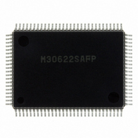
M30622SAFP#U5 Renesas Electronics America, M30622SAFP#U5 Datasheet - Page 544

M30622SAFP#U5
Manufacturer Part Number
M30622SAFP#U5
Description
IC M16C MPU ROMLESS 100QFP
Manufacturer
Renesas Electronics America
Series
M16C™ M16C/60r
Datasheets
1.QSK-62P_PLUS.pdf
(103 pages)
2.M30622SAFPU5.pdf
(277 pages)
3.M30622SAFPU5.pdf
(617 pages)
4.M30622SAFPU5.pdf
(308 pages)
Specifications of M30622SAFP#U5
Core Processor
M16C/60
Core Size
16-Bit
Speed
16MHz
Connectivity
SIO, UART/USART
Peripherals
DMA, PWM, WDT
Number Of I /o
50
Program Memory Type
ROMless
Ram Size
3K x 8
Voltage - Supply (vcc/vdd)
4.2 V ~ 5.5 V
Data Converters
A/D 10x10b, D/A 2x8b
Oscillator Type
Internal
Operating Temperature
-20°C ~ 85°C
Package / Case
100-QFP
For Use With
867-1000 - KIT QUICK START RENESAS 62PM3062PT3-CPE-3 - EMULATOR COMPACT M16C/62P/30P
Lead Free Status / RoHS Status
Lead free / RoHS Compliant
Eeprom Size
-
Program Memory Size
-
Available stocks
Company
Part Number
Manufacturer
Quantity
Price
- QSK-62P_PLUS PDF datasheet
- M30622SAFPU5 PDF datasheet #2
- M30622SAFPU5 PDF datasheet #3
- M30622SAFPU5 PDF datasheet #4
- Current page: 544 of 617
- Download datasheet (9Mb)
External Buses
Figure 4.2.3. Chip select control register
4.2.3 Bus Types
4.2.4 R/W Modes
The M16C/62A Group has two types of buses: a separate bus where separate pins are used for address
output and data input/output and a multiplexed bus where pins are time- multiplexed and switched be-
tween address output and data input/output to save the number of pins used.
A separate bus is used to access devices such as ROM and RAM which have separate buses. The areas
accessed via separate buses can be allocated for programs and data.
A multiplexed bus is used to access devices such as ASSPs which have multiplexed buses. The areas
accessed via a multiplexed bus can only be allocated for data. Programs cannot be located in these areas.
The area accessed via a multiplex bus can be selected from three types of area CS2 area, CS1 area, and
entire space by setting the multiplexed bus select bits (bits 4 and 5) of the processor mode register 0 (address
0004
Areas not accessed via multiplexed bus are accessed through separate buses.
When accessing an area set for access via a multiplexed bus the BYTE pin is “H” level, the data bus D
to D
If the BYTE pin is “L” level, the data bus D
the bus is switched between data and address separated only in time.
In the latter case, however, the addresses of connected devices are mapped into even addresses (every
other addresses) of the M16C/62A. Therefore, be sure to access the M16C/62A's even addresses in
length of bytes when accessing a connected device.
The read/write signal that is output when accessing an external area can be selected between the RD/
BHE/WR and the RD/WRH/WRL modes by setting the R/W mode select bit (bit 2) of the processor mode
register 0 (address 0004
________
WRL mode to access an 8-bit wide RAM.
When the M16C/62A is reset, the RD/BHE/WR mode is selected by default. To switch over the R/W
mode, change the RD/BHE/WR to the RD/WRH/WRL mode before accessing an external RAM.
Refer to the connection examples of RD/BHE/WR and RD/WRH/WRL shown in Section 4.3, "Connection
Examples."
_______ ______
7
16
Chip select control register
is multiplexed with address bus A
). However, the entire space cannot be selected when operating in the microprocessor mode.
b7
b6
b5
b4
b3
_____ _________ ________
_____ ________ ______
b2
b1
16
b0
). Use the RD/BHE/WR mode to access a 16-bit wide RAM and the RD/WRH/
Bit symbol
CS0
CS1
CS2
CS3
CS0W
CS1W
CS2W
CS3W
Symbol
CSR
_____ ________ ______
_____ ________ ______
_____ ________ ______
CS0 output enable bit
CS1 output enable bit
CS2 output enable bit
CS3 output enable bit
CS0 wait bit
CS1 wait bit
CS2 wait bit
CS3 wait bit
_____ _________ ________
0
to A
0
to D
Bit name
7
.
7
Address
0008
is multiplexed with address bus A
16
_____ _________ ________
When reset
0 : Chip select output disabled
1 : Chip select output enabled
0 : Wait state inserted
1 : No wait state
01
(Normal port pin)
16
SINGLE-CHIP 16-BIT CMOS MICROCOMPUTER
Function
_______
1
to A
M16C / 62A Group
R
Mitsubishi microcomputers
W
8
. In either case,
______
_____ _________
2-225
_____
0
Related parts for M30622SAFP#U5
Image
Part Number
Description
Manufacturer
Datasheet
Request
R

Part Number:
Description:
KIT STARTER FOR M16C/29
Manufacturer:
Renesas Electronics America
Datasheet:

Part Number:
Description:
KIT STARTER FOR R8C/2D
Manufacturer:
Renesas Electronics America
Datasheet:

Part Number:
Description:
R0K33062P STARTER KIT
Manufacturer:
Renesas Electronics America
Datasheet:

Part Number:
Description:
KIT STARTER FOR R8C/23 E8A
Manufacturer:
Renesas Electronics America
Datasheet:

Part Number:
Description:
KIT STARTER FOR R8C/25
Manufacturer:
Renesas Electronics America
Datasheet:

Part Number:
Description:
KIT STARTER H8S2456 SHARPE DSPLY
Manufacturer:
Renesas Electronics America
Datasheet:

Part Number:
Description:
KIT STARTER FOR R8C38C
Manufacturer:
Renesas Electronics America
Datasheet:

Part Number:
Description:
KIT STARTER FOR R8C35C
Manufacturer:
Renesas Electronics America
Datasheet:

Part Number:
Description:
KIT STARTER FOR R8CL3AC+LCD APPS
Manufacturer:
Renesas Electronics America
Datasheet:

Part Number:
Description:
KIT STARTER FOR RX610
Manufacturer:
Renesas Electronics America
Datasheet:

Part Number:
Description:
KIT STARTER FOR R32C/118
Manufacturer:
Renesas Electronics America
Datasheet:

Part Number:
Description:
KIT DEV RSK-R8C/26-29
Manufacturer:
Renesas Electronics America
Datasheet:

Part Number:
Description:
KIT STARTER FOR SH7124
Manufacturer:
Renesas Electronics America
Datasheet:

Part Number:
Description:
KIT STARTER FOR H8SX/1622
Manufacturer:
Renesas Electronics America
Datasheet:

Part Number:
Description:
KIT DEV FOR SH7203
Manufacturer:
Renesas Electronics America
Datasheet:


