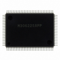
M30622SAFP#U5 Renesas Electronics America, M30622SAFP#U5 Datasheet - Page 94

M30622SAFP#U5
Manufacturer Part Number
M30622SAFP#U5
Description
IC M16C MPU ROMLESS 100QFP
Manufacturer
Renesas Electronics America
Series
M16C™ M16C/60r
Datasheets
1.QSK-62P_PLUS.pdf
(103 pages)
2.M30622SAFPU5.pdf
(277 pages)
3.M30622SAFPU5.pdf
(617 pages)
4.M30622SAFPU5.pdf
(308 pages)
Specifications of M30622SAFP#U5
Core Processor
M16C/60
Core Size
16-Bit
Speed
16MHz
Connectivity
SIO, UART/USART
Peripherals
DMA, PWM, WDT
Number Of I /o
50
Program Memory Type
ROMless
Ram Size
3K x 8
Voltage - Supply (vcc/vdd)
4.2 V ~ 5.5 V
Data Converters
A/D 10x10b, D/A 2x8b
Oscillator Type
Internal
Operating Temperature
-20°C ~ 85°C
Package / Case
100-QFP
For Use With
867-1000 - KIT QUICK START RENESAS 62PM3062PT3-CPE-3 - EMULATOR COMPACT M16C/62P/30P
Lead Free Status / RoHS Status
Lead free / RoHS Compliant
Eeprom Size
-
Program Memory Size
-
Available stocks
Company
Part Number
Manufacturer
Quantity
Price
- QSK-62P_PLUS PDF datasheet
- M30622SAFPU5 PDF datasheet #2
- M30622SAFPU5 PDF datasheet #3
- M30622SAFPU5 PDF datasheet #4
- Current page: 94 of 617
- Download datasheet (9Mb)
DMAC
(1) Transfer cycle
The transfer cycle consists of the bus cycle in which data is read from memory or from the SFR area
(source read) and the bus cycle in which the data is written to memory or to the SFR area (destination
write). The number of read and write bus cycles depends on the source and destination addresses. In
memory expansion mode and microprocessor mode, the number of read and write bus cycles also de-
pends on the level of the BYTE pin. Also, the bus cycle itself is longer when software waits are inserted.
Figure 1.13.5 shows the example of the transfer cycles for a source read. For convenience, the destina-
tion write cycle is shown as one cycle and the source read cycles for the different conditions are shown.
In reality, the destination write cycle is subject to the same conditions as the source read cycle, with the
transfer cycle changing accordingly. When calculating the transfer cycle, remember to apply the respec-
tive conditions to both the destination write cycle and the source read cycle. For example (2) in Figure
1.13.5, if data is being transferred in 16-bit units on an 8-bit bus, two bus cycles are required for both the
source read cycle and the destination write cycle.
(a) Effect of source and destination addresses
(b) Effect of BYTE pin level
(c) Effect of software wait
When 16-bit data is transferred on a 16-bit data bus, and the source and destination both start at odd
addresses, there are one more source read cycle and destination write cycle than when the source
and destination both start at even addresses.
When transferring 16-bit data over an 8-bit data bus (BYTE pin = “H”) in memory expansion mode and
microprocessor mode, the 16 bits of data are sent in two 8-bit blocks. Therefore, two bus cycles are
required for reading the data and two are required for writing the data. Also, in contrast to when the
CPU accesses internal memory, when the DMAC accesses internal memory (internal ROM, internal
RAM, and SFR), these areas are accessed using the data size selected by the BYTE pin.
When the SFR area or a memory area with a software wait is accessed, the number of cycles is
increased for the wait by 1 bus cycle. The length of the cycle is determined by BCLK.
SINGLE-CHIP 16-BIT CMOS MICROCOMPUTER
M16C / 62A Group
Mitsubishi microcomputers
1-73
Related parts for M30622SAFP#U5
Image
Part Number
Description
Manufacturer
Datasheet
Request
R

Part Number:
Description:
KIT STARTER FOR M16C/29
Manufacturer:
Renesas Electronics America
Datasheet:

Part Number:
Description:
KIT STARTER FOR R8C/2D
Manufacturer:
Renesas Electronics America
Datasheet:

Part Number:
Description:
R0K33062P STARTER KIT
Manufacturer:
Renesas Electronics America
Datasheet:

Part Number:
Description:
KIT STARTER FOR R8C/23 E8A
Manufacturer:
Renesas Electronics America
Datasheet:

Part Number:
Description:
KIT STARTER FOR R8C/25
Manufacturer:
Renesas Electronics America
Datasheet:

Part Number:
Description:
KIT STARTER H8S2456 SHARPE DSPLY
Manufacturer:
Renesas Electronics America
Datasheet:

Part Number:
Description:
KIT STARTER FOR R8C38C
Manufacturer:
Renesas Electronics America
Datasheet:

Part Number:
Description:
KIT STARTER FOR R8C35C
Manufacturer:
Renesas Electronics America
Datasheet:

Part Number:
Description:
KIT STARTER FOR R8CL3AC+LCD APPS
Manufacturer:
Renesas Electronics America
Datasheet:

Part Number:
Description:
KIT STARTER FOR RX610
Manufacturer:
Renesas Electronics America
Datasheet:

Part Number:
Description:
KIT STARTER FOR R32C/118
Manufacturer:
Renesas Electronics America
Datasheet:

Part Number:
Description:
KIT DEV RSK-R8C/26-29
Manufacturer:
Renesas Electronics America
Datasheet:

Part Number:
Description:
KIT STARTER FOR SH7124
Manufacturer:
Renesas Electronics America
Datasheet:

Part Number:
Description:
KIT STARTER FOR H8SX/1622
Manufacturer:
Renesas Electronics America
Datasheet:

Part Number:
Description:
KIT DEV FOR SH7203
Manufacturer:
Renesas Electronics America
Datasheet:


