MC9S12E256MFUE Freescale Semiconductor, MC9S12E256MFUE Datasheet - Page 553
MC9S12E256MFUE
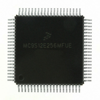
Manufacturer Part Number
MC9S12E256MFUE
Description
IC MCU 256K FLASH 25MHZ 80-QFP
Manufacturer
Freescale Semiconductor
Series
HCS12r
Specifications of MC9S12E256MFUE
Core Processor
HCS12
Core Size
16-Bit
Speed
25MHz
Connectivity
EBI/EMI, I²C, SCI, SPI
Peripherals
POR, PWM, WDT
Number Of I /o
60
Program Memory Size
256KB (256K x 8)
Program Memory Type
FLASH
Ram Size
16K x 8
Voltage - Supply (vcc/vdd)
2.35 V ~ 2.75 V
Data Converters
A/D 16x10b; D/A 2x8b
Oscillator Type
Internal
Operating Temperature
-40°C ~ 125°C
Package / Case
80-QFP
Processor Series
S12E
Core
HCS12
Data Bus Width
16 bit
Data Ram Size
16 KB
Interface Type
I2C/SCI/SPI
Maximum Clock Frequency
50 MHz
Number Of Programmable I/os
60
Number Of Timers
12
Operating Supply Voltage
0 V to 5 V
Maximum Operating Temperature
+ 125 C
Mounting Style
SMD/SMT
3rd Party Development Tools
EWHCS12
Minimum Operating Temperature
- 40 C
On-chip Adc
16-ch x 10-bit
On-chip Dac
2-ch x 8-bit
Controller Family/series
HCS12/S12X
No. Of I/o's
60
Ram Memory Size
16KB
Cpu Speed
25MHz
No. Of Timers
3
Embedded Interface Type
I2C, SCI, SPI
Rohs Compliant
Yes
For Use With
M68EVB912E128 - BOARD EVAL FOR MC9S12E128/64
Lead Free Status / RoHS Status
Lead free / RoHS Compliant
Eeprom Size
-
Lead Free Status / Rohs Status
Lead free / RoHS Compliant
Available stocks
Company
Part Number
Manufacturer
Quantity
Price
Company:

Part Number:
MC9S12E256MFUE
Manufacturer:
FREESCAL
Quantity:
329
Company:
Part Number:
MC9S12E256MFUE
Manufacturer:
Freescale Semiconductor
Quantity:
10 000


of data flow from the CPU to the output address and data buses of the core. In addition, the MMC manages
all CPU read data bus swapping operations.
19.4.2
As data flows on the core address bus, the MMC decodes the address information, determines whether the
internal core register or firmware space, the peripheral space or a memory register or array space is being
addressed and generates the correct select signal. This decoding operation also interprets the mode of
operation of the system and the state of the mapping control registers in order to generate the proper select.
The MMC also generates two external chip select signals, emulation chip select (ECS) and external chip
select (XCS).
19.4.2.1
Although internal resources such as control registers and on-chip memory have default addresses, each can
be relocated by changing the default values in control registers. Normally, I/O addresses, control registers,
vector spaces, expansion windows, and on-chip memory are mapped so that their address ranges do not
overlap. The MMC will make only one select signal active at any given time. This activation is based upon
the priority outlined in
signal for the block with the highest priority will become active. An example of this is if the registers and
the RAM are mapped to the same space, the registers will have priority over the RAM and the portion of
RAM mapped in this shared space will not be accessible. The expansion windows have the lowest priority.
This means that registers, vectors, and on-chip memory are always visible to a program regardless of the
values in the page select registers.
In expanded modes, all address space not used by internal resources is by default external memory space.
The data registers and data direction registers for ports A and B are removed from the on-chip memory
map and become external accesses. If the EME bit in the MODE register (see
External Bus Interface
from the on-chip memory map and become external accesses.
In special peripheral mode, the first 16 registers associated with bus expansion are removed from the
on-chip memory map (PORTA, PORTB, DDRA, DDRB, PORTE, DDRE, PEAR, MODE, PUCR,
RDRIV, and the EBI reserved registers).
Freescale Semiconductor
Address Decoding
Select Priority and Mode Considerations
(MEBIV3)”) is set, the data and data direction registers for port E are also removed
Table
Priority
Highest
Lowest
...
...
...
...
19-15. If two or more blocks share the same address space, only the select
Table 19-15. Select Signal Priority
MC9S12E256 Data Sheet, Rev. 1.08
BDM (internal to core) firmware or register space
Remaining external space
EEPROM memory block
On-chip FLASH or ROM
Internal register space
RAM memory block
Address Space
Chapter 19 Module Mapping Control (MMCV4)
Chapter 18, “Multiplexed
553
Related parts for MC9S12E256MFUE
Image
Part Number
Description
Manufacturer
Datasheet
Request
R

Part Number:
Description:
Manufacturer:
Freescale Semiconductor, Inc
Datasheet:
Part Number:
Description:
Manufacturer:
Freescale Semiconductor, Inc
Datasheet:
Part Number:
Description:
Manufacturer:
Freescale Semiconductor, Inc
Datasheet:
Part Number:
Description:
Manufacturer:
Freescale Semiconductor, Inc
Datasheet:
Part Number:
Description:
Manufacturer:
Freescale Semiconductor, Inc
Datasheet:
Part Number:
Description:
Manufacturer:
Freescale Semiconductor, Inc
Datasheet:
Part Number:
Description:
Manufacturer:
Freescale Semiconductor, Inc
Datasheet:
Part Number:
Description:
Manufacturer:
Freescale Semiconductor, Inc
Datasheet:
Part Number:
Description:
Manufacturer:
Freescale Semiconductor, Inc
Datasheet:
Part Number:
Description:
Manufacturer:
Freescale Semiconductor, Inc
Datasheet:
Part Number:
Description:
Manufacturer:
Freescale Semiconductor, Inc
Datasheet:
Part Number:
Description:
Manufacturer:
Freescale Semiconductor, Inc
Datasheet:
Part Number:
Description:
Manufacturer:
Freescale Semiconductor, Inc
Datasheet:
Part Number:
Description:
Manufacturer:
Freescale Semiconductor, Inc
Datasheet:
Part Number:
Description:
Manufacturer:
Freescale Semiconductor, Inc
Datasheet: