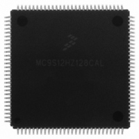
MC9S12HZ128CAL Freescale Semiconductor, MC9S12HZ128CAL Datasheet - Page 250

MC9S12HZ128CAL
Manufacturer Part Number
MC9S12HZ128CAL
Description
IC MCU 16BIT 128K FLASH 112-LQFP
Manufacturer
Freescale Semiconductor
Series
HCS12r
Datasheet
1.MC9S12HZ128CAL.pdf
(692 pages)
Specifications of MC9S12HZ128CAL
Core Processor
HCS12
Core Size
16-Bit
Speed
25MHz
Connectivity
CAN, EBI/EMI, I²C, SCI, SPI
Peripherals
LCD, Motor control PWM, POR, PWM, WDT
Number Of I /o
85
Program Memory Size
128KB (128K x 8)
Program Memory Type
FLASH
Eeprom Size
2K x 8
Ram Size
6K x 8
Voltage - Supply (vcc/vdd)
2.35 V ~ 5.5 V
Data Converters
A/D 16x10b
Oscillator Type
Internal
Operating Temperature
-40°C ~ 85°C
Package / Case
112-LQFP
Processor Series
S12H
Core
HCS12
Data Bus Width
16 bit
Data Ram Size
6 KB
Interface Type
I2C, SCI, SPI
Maximum Clock Frequency
50 MHz
Number Of Programmable I/os
85
Number Of Timers
8
Maximum Operating Temperature
+ 85 C
Mounting Style
SMD/SMT
3rd Party Development Tools
EWHCS12
Minimum Operating Temperature
- 40 C
On-chip Adc
10 bit, 16 Channel
Lead Free Status / RoHS Status
Lead free / RoHS Compliant
Available stocks
Company
Part Number
Manufacturer
Quantity
Price
Company:
Part Number:
MC9S12HZ128CAL
Manufacturer:
Freescale Semiconductor
Quantity:
10 000
- Current page: 250 of 692
- Download datasheet (4Mb)
Chapter 8 Liquid Crystal Display (LCD32F4BV1)
8.4.1.3
For a segment on the LCD to be displayed, data must be written to the LCD RAM which is shown in
Section 8.3, “Memory Map and Register
segments that are driven by the frontplane and backplane drivers. Writing a 1 to a given location will result
in the corresponding display segment being driven with a differential RMS voltage necessary to turn the
segment ON when the LCDEN bit is set and the corresponding FP[31:0]EN bit is set. Writing a 0 to a given
location will result in the corresponding display segment being driven with a differential RMS voltage
necessary to turn the segment OFF. The LCD RAM is a dual port RAM that interfaces with the internal
address and data buses of the MCU. It is possible to read from LCD RAM locations for scrolling purposes.
When LCDEN = 0, the LCD RAM can be used as on-chip RAM. Writing or reading of the LCDEN bit
does not change the contents of the LCD RAM. After a reset, the LCD RAM contents will be
indeterminate.
8.4.1.4
If LCDEN = 0 (LCD32F4B driver system disabled) and the frontplane enable bit, FP[31:0]EN, is set, the
frontplane driver waveform will not appear on the output until LCDEN is set. If LCDEN = 1 (LCD32F4B
driver system enabled), the frontplane driver waveform will appear on the output as soon as the
corresponding frontplane enable bit, FP[31:0]EN, in the registers FPENR0–FPENR3 is set.
8.4.1.5
The LCD32F4B driver has five modes of operation:
The voltage levels required for the different operating modes are generated internally based on VLCD.
Changing VLCD alters the differential RMS voltage across the segments in the ON and OFF states,
thereby setting the display contrast.
The backplane waveforms are continuous and repetitive every frame. They are fixed within each operating
mode and are not affected by the data in the LCD RAM.
The frontplane waveforms generated are dependent on the state (ON or OFF) of the LCD segments as
defined in the LCD RAM. The LCD32F4B driver hardware uses the data in the LCD RAM to construct
the frontplane waveform to create a differential RMS voltage necessary to turn the segment ON or OFF.
The LCD duty is decided by the DUTY1 and DUTY0 bits in the LCD control register 0 (LCDCR0). The
number of bias voltage levels is determined by the BIAS bit in LCDCR0.
multiplex modes (duties) and the bias voltage levels that can be selected for each multiplex mode (duty).
The backplane pins have their corresponding backplane waveform output BP[3:0] in high impedance state
when in the OFF state as indicated in
used for other functionality, for example as general purpose I/O ports.
250
•
•
•
•
•
1/1 duty (1 backplane), 1/1 bias (2 voltage levels)
1/2 duty (2 backplanes), 1/2 bias (3 voltage levels)
1/2 duty (2 backplanes), 1/3 bias (4 voltage levels)
1/3 duty (3 backplanes), 1/3 bias (4 voltage levels)
1/4 duty (4 backplanes), 1/3 bias (4 voltage levels)
LCD RAM
LCD Driver System Enable and Frontplane Enable Sequencing
LCD Bias and Modes of Operation
MC9S12HZ256 Data Sheet, Rev. 2.05
Table
Definition”. The 128 bits in the LCD RAM correspond to the 128
8-8. In the OFF state the corresponding pins BP[3:0]can be
Table 8-8
Freescale Semiconductor
summarizes the
Related parts for MC9S12HZ128CAL
Image
Part Number
Description
Manufacturer
Datasheet
Request
R
Part Number:
Description:
Manufacturer:
Freescale Semiconductor, Inc
Datasheet:
Part Number:
Description:
Manufacturer:
Freescale Semiconductor, Inc
Datasheet:
Part Number:
Description:
Manufacturer:
Freescale Semiconductor, Inc
Datasheet:
Part Number:
Description:
Manufacturer:
Freescale Semiconductor, Inc
Datasheet:
Part Number:
Description:
Manufacturer:
Freescale Semiconductor, Inc
Datasheet:
Part Number:
Description:
Manufacturer:
Freescale Semiconductor, Inc
Datasheet:
Part Number:
Description:
Manufacturer:
Freescale Semiconductor, Inc
Datasheet:
Part Number:
Description:
Manufacturer:
Freescale Semiconductor, Inc
Datasheet:
Part Number:
Description:
Manufacturer:
Freescale Semiconductor, Inc
Datasheet:
Part Number:
Description:
Manufacturer:
Freescale Semiconductor, Inc
Datasheet:
Part Number:
Description:
Manufacturer:
Freescale Semiconductor, Inc
Datasheet:
Part Number:
Description:
Manufacturer:
Freescale Semiconductor, Inc
Datasheet:
Part Number:
Description:
Manufacturer:
Freescale Semiconductor, Inc
Datasheet:
Part Number:
Description:
Manufacturer:
Freescale Semiconductor, Inc
Datasheet:
Part Number:
Description:
Manufacturer:
Freescale Semiconductor, Inc
Datasheet:


