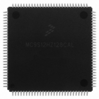
MC9S12HZ128CAL Freescale Semiconductor, MC9S12HZ128CAL Datasheet - Page 632

MC9S12HZ128CAL
Manufacturer Part Number
MC9S12HZ128CAL
Description
IC MCU 16BIT 128K FLASH 112-LQFP
Manufacturer
Freescale Semiconductor
Series
HCS12r
Datasheet
1.MC9S12HZ128CAL.pdf
(692 pages)
Specifications of MC9S12HZ128CAL
Core Processor
HCS12
Core Size
16-Bit
Speed
25MHz
Connectivity
CAN, EBI/EMI, I²C, SCI, SPI
Peripherals
LCD, Motor control PWM, POR, PWM, WDT
Number Of I /o
85
Program Memory Size
128KB (128K x 8)
Program Memory Type
FLASH
Eeprom Size
2K x 8
Ram Size
6K x 8
Voltage - Supply (vcc/vdd)
2.35 V ~ 5.5 V
Data Converters
A/D 16x10b
Oscillator Type
Internal
Operating Temperature
-40°C ~ 85°C
Package / Case
112-LQFP
Processor Series
S12H
Core
HCS12
Data Bus Width
16 bit
Data Ram Size
6 KB
Interface Type
I2C, SCI, SPI
Maximum Clock Frequency
50 MHz
Number Of Programmable I/os
85
Number Of Timers
8
Maximum Operating Temperature
+ 85 C
Mounting Style
SMD/SMT
3rd Party Development Tools
EWHCS12
Minimum Operating Temperature
- 40 C
On-chip Adc
10 bit, 16 Channel
Lead Free Status / RoHS Status
Lead free / RoHS Compliant
Available stocks
Company
Part Number
Manufacturer
Quantity
Price
Company:
Part Number:
MC9S12HZ128CAL
Manufacturer:
Freescale Semiconductor
Quantity:
10 000
- Current page: 632 of 692
- Download datasheet (4Mb)
1
2
Appendix A Electrical Characteristics
A.2
This section describes the characteristics of the analog to digital converter.
A.2.1
The
The following constraints exist to obtain full-scale, full range results:
V
beyond the power supply levels that it ties to. If the input level goes outside of this range it will effectively
be clipped.
A.2.2
Three factors – source resistance, source capacitance and current injection – have an influence on the
accuracy of the ATD.
A.2.2.1
Due to the input pin leakage current as specified in
there will be a voltage drop from the signal source to the ATD input. The maximum source resistance R
specifies results in an error of less than 1/2 LSB (2.5mV) at the maximum leakage current. If device or
operating conditions are less than worst case or leakage-induced error is acceptable, larger values of source
resistance is allowed.
632
Conditions are shown in
Num C
Full accuracy is not guaranteed when differential voltage is less than 4.50V
The minimum time assumes a final sample period of 2 ATD clocks cycles while the maximum time assumes a final sample
period of 16 ATD clocks.
SSA
1
2
3
4
5
6
7
Table A-8
D Reference Potential
C Differential Reference Voltage
D ATD Clock Frequency
D ATD 10-Bit Conversion Period
D ATD 8-Bit Conversion Period
D Stop Recovery Time (V
P Reference Supply current
V
ATD
RL
ATD Operating Characteristics
Factors influencing accuracy
Source Resistance:
shows conditions under which the ATD operates.
V
IN
Conv, Time at 2.0MHz ATD Clock f
Conv, Time at 2.0MHz ATD Clock f
Table A-4
V
RH
Rating
DDA
V
unless otherwise noted
DDA
=5.0 Volts)
Table A-8. ATD Operating Characteristics
1
This constraint exists since the sample buffer amplifier can not drive
MC9S12HZ256 Data Sheet, Rev. 2.05
Clock Cycles
Clock Cycles
ATDCLK
ATDCLK
High
Low
Table A-6
2
2
V
N
T
Symbol
N
f
T
RH
ATDCLK
CONV10
CONV10
CONV8
CONV8
V
I
V
t
REF
SR
RH
RL
–V
RL
in conjunction with the source resistance
V
V
4.50
DDA
Min
0.5
14
12
SSA
7
6
/2
5.00
Typ
Freescale Semiconductor
V
0.375
V
Max
5.25
DDA
2.0
28
14
26
13
20
DDA
/2
Cycles
Cycles
MHz
Unit
mA
V
V
V
s
s
s
S
Related parts for MC9S12HZ128CAL
Image
Part Number
Description
Manufacturer
Datasheet
Request
R
Part Number:
Description:
Manufacturer:
Freescale Semiconductor, Inc
Datasheet:
Part Number:
Description:
Manufacturer:
Freescale Semiconductor, Inc
Datasheet:
Part Number:
Description:
Manufacturer:
Freescale Semiconductor, Inc
Datasheet:
Part Number:
Description:
Manufacturer:
Freescale Semiconductor, Inc
Datasheet:
Part Number:
Description:
Manufacturer:
Freescale Semiconductor, Inc
Datasheet:
Part Number:
Description:
Manufacturer:
Freescale Semiconductor, Inc
Datasheet:
Part Number:
Description:
Manufacturer:
Freescale Semiconductor, Inc
Datasheet:
Part Number:
Description:
Manufacturer:
Freescale Semiconductor, Inc
Datasheet:
Part Number:
Description:
Manufacturer:
Freescale Semiconductor, Inc
Datasheet:
Part Number:
Description:
Manufacturer:
Freescale Semiconductor, Inc
Datasheet:
Part Number:
Description:
Manufacturer:
Freescale Semiconductor, Inc
Datasheet:
Part Number:
Description:
Manufacturer:
Freescale Semiconductor, Inc
Datasheet:
Part Number:
Description:
Manufacturer:
Freescale Semiconductor, Inc
Datasheet:
Part Number:
Description:
Manufacturer:
Freescale Semiconductor, Inc
Datasheet:
Part Number:
Description:
Manufacturer:
Freescale Semiconductor, Inc
Datasheet:


