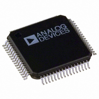
ADUC7128BSTZ126-RL Analog Devices Inc, ADUC7128BSTZ126-RL Datasheet - Page 52

ADUC7128BSTZ126-RL
Manufacturer Part Number
ADUC7128BSTZ126-RL
Description
IC DAS MCU ARM7 ADC/DDS 64-LQFP
Manufacturer
Analog Devices Inc
Series
MicroConverter® ADuC7xxxr
Datasheet
1.EVAL-ADUC7128QSPZ.pdf
(92 pages)
Specifications of ADUC7128BSTZ126-RL
Core Size
16/32-Bit
Program Memory Size
126KB (126K x 8)
Core Processor
ARM7
Speed
41.78MHz
Connectivity
I²C, SPI, UART/USART
Peripherals
PLA, POR, PWM, PSM, Temp Sensor, WDT
Number Of I /o
28
Program Memory Type
FLASH
Ram Size
8K x 8
Voltage - Supply (vcc/vdd)
3 V ~ 3.6 V
Data Converters
A/D 10x12b; D/A 1x10b
Oscillator Type
Internal
Operating Temperature
-40°C ~ 125°C
Package / Case
64-LQFP
Controller Family/series
(ARM7) ADUC
No. Of I/o's
40
Cpu Speed
41.78MHz
No. Of Timers
5
Digital Ic Case Style
LQFP
Embedded Interface Type
I2C, SPI, UART
Rohs Compliant
Yes
Lead Free Status / RoHS Status
Lead free / RoHS Compliant
For Use With
EVAL-ADUC7128QSPZ - KIT DEV FOR ADUC7128
Eeprom Size
-
Lead Free Status / RoHS Status
Lead free / RoHS Compliant, Lead free / RoHS Compliant
Other names
ADUC7128BSTZ126-RLTR
Available stocks
Company
Part Number
Manufacturer
Quantity
Price
Company:
Part Number:
ADUC7128BSTZ126-RL
Manufacturer:
Analog Devices Inc
Quantity:
10 000
ADuC7128/ADuC7129
Bit
6
5
4
3
2
1
0
In H-bridge mode, HMODE = 1. See Table 65 to determine the PWM outputs.
Table 65. PWM Output Selection
ENA
0
x
1
1
1
1
1
On power-up, PWMCON1 defaults to 0x12 (HOFF = 1 and
HMODE = 1). All GPIO pins associated with the PWM are
configured in PWM mode by default (see Table 66).
Table 66. Compare Register
Name
PWM1COM1
PWM1COM2
PWM1COM3
PWM2COM1
PWM2COM2
PWM2COM3
PWM3COM1
PWM3COM2
PWM3COM3
HS = high side, LS = low side.
PWMCOM1 MMR
Name
POINV
HOFF
LCOMP
DIR
HMODE
PWMEN
PWMCP0
HOFF
0
1
0
0
0
0
POINV
x
x
0
0
1
1
Address
0xFFFF0F84
0xFFFF0F88
0xFFFF0F8C
0xFFFF0F94
0xFFFF0F98
0xFFFF0F9C
0xFFFF0FA4
0xFFFF0FA8
0xFFFF0FAC
Description
2.
4.
8.
16.
32.
64.
128.
256.
Set to 1 by the user to invert all PWM outputs.
Cleared by user to use PWM outputs as normal.
High Side Off.
Load Compare Registers.
Direction Control.
Enables H-bridge mode.
Set to 1 by the user to enable all PWM outputs.
Cleared by user to disable all PWM outputs.
Set to 1 by the user to force PWM1 and PWM3 outputs high. This also forces PWM2 and PWM4 low.
Cleared by user to use the PWM outputs as normal.
Set to 1 by the user to load the internal compare registers with the values in PWMxCOMx on the next transition of the
PWM timer from 0x00 to 0x01.
Cleared by user to use the values previously stored in the internal compare registers.
Set to 1 by the user to enable PWM1 and PWM2 as the output signals while PWM3 and PWM4 are held low.
Cleared by user to enable PWM3 and PWM4 as the output signals while PWM1 and PWM2 are held low.
Set to 1 by the user to enable H-Bridge mode and Bit 1 to Bit 5 of PWMCON1.
Cleared by user to operate the PWMs in standard mode.
DIR
x
x
0
1
0
1
PWM1
1
1
0
HS
HS
1
1
1
Default Value
0x00
0x00
0x00
0x00
0x00
0x00
0x00
0x00
0x00
PWM2
1
0
0
LS
LS
1
PWM Outputs
1
1
PWMR3
1
1
HS
0
1
HS
1
1
Access
R/W
R/W
R/W
R/W
R/W
R/W
R/W
R/W
R/W
PWM4
1
0
LS
0
1
LS
1
1
Rev. 0 | Page 52 of 92
The PWM trip interrupt can be cleared by writing any value to
the PWMICLR MMR. Note that when using the PWM trip
interrupt, the PWM interrupt should be cleared before exiting
the ISR. This prevents generation of multiple interrupts.
PWM CONVERT START CONTROL
The PWM can be configured to generate an ADC convert start
signal after the active low side signal goes high. There is a program-
mable delay between when the low-side signal goes high and
the convert start signal is generated.
This is controlled via the PWMCON2 MMR. If the delay
selected is higher than the width of the PWM pulse, the
interrupt remains low.


