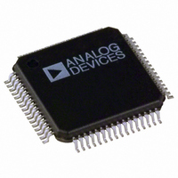
ADUC7128BSTZ126-RL Analog Devices Inc, ADUC7128BSTZ126-RL Datasheet - Page 57

ADUC7128BSTZ126-RL
Manufacturer Part Number
ADUC7128BSTZ126-RL
Description
IC DAS MCU ARM7 ADC/DDS 64-LQFP
Manufacturer
Analog Devices Inc
Series
MicroConverter® ADuC7xxxr
Datasheet
1.EVAL-ADUC7128QSPZ.pdf
(92 pages)
Specifications of ADUC7128BSTZ126-RL
Core Size
16/32-Bit
Program Memory Size
126KB (126K x 8)
Core Processor
ARM7
Speed
41.78MHz
Connectivity
I²C, SPI, UART/USART
Peripherals
PLA, POR, PWM, PSM, Temp Sensor, WDT
Number Of I /o
28
Program Memory Type
FLASH
Ram Size
8K x 8
Voltage - Supply (vcc/vdd)
3 V ~ 3.6 V
Data Converters
A/D 10x12b; D/A 1x10b
Oscillator Type
Internal
Operating Temperature
-40°C ~ 125°C
Package / Case
64-LQFP
Controller Family/series
(ARM7) ADUC
No. Of I/o's
40
Cpu Speed
41.78MHz
No. Of Timers
5
Digital Ic Case Style
LQFP
Embedded Interface Type
I2C, SPI, UART
Rohs Compliant
Yes
Lead Free Status / RoHS Status
Lead free / RoHS Compliant
For Use With
EVAL-ADUC7128QSPZ - KIT DEV FOR ADUC7128
Eeprom Size
-
Lead Free Status / RoHS Status
Lead free / RoHS Compliant, Lead free / RoHS Compliant
Other names
ADUC7128BSTZ126-RLTR
Available stocks
Company
Part Number
Manufacturer
Quantity
Price
Company:
Part Number:
ADUC7128BSTZ126-RL
Manufacturer:
Analog Devices Inc
Quantity:
10 000
GPxDAT Register
Name
GP0DAT
GP1DAT
GP2DAT
GP3DAT
GP4DAT
GPxDAT is a Port x configuration and data register. It configures
the direction of the GPIO pins of Port x, sets the output value
for the pins configured as output, and receives and stores the
input value of the pins configured as input.
Table 73. GPxDAT MMR Bit Designations
Bit
31:24
23:16
15:8
7:0
GPxSET Register
Name
GP0SET
GP1SET
GP2SET
GP3SET
GP4SET
GPxSET is a data set Port x register.
Table 74. GPxSET MMR Bit Designations
Bit
31:24
23:16
15:0
GPxCLR Register
Name
GP0CLR
GP1CLR
GP2CLR
GP3CLR
GP4CLR
GPxCLR is a data clear Port x register.
Table 75. GPxCLR MMR Bit Designations
Bit
31:24
23:16
15:0
Description
Reserved.
Data Port x Set Bit.
Reserved.
Description
Direction of the Data.
Port x Data Output.
Reflect the state of Port x pins at reset (read only).
Port x Data Input (Read Only).
Description
Reserved.
Data Port x Clear Bit.
Reserved.
Set to 1 by user to set bit on Port x; also sets the
corresponding bit in the GPxDAT MMR.
Cleared to 0 by user; does not affect the data out.
Set to 1 by user to configure the GPIO pins as outputs.
Cleared to 0 by user to configure the GPIO pins as
inputs.
Set to 1 by user to clear bit on Port x; also clears
the corresponding bit in the GPxDAT MMR.
Cleared to 0 by user; does not affect the data out.
Address
0xFFFF0D20
0xFFFF0D30
0xFFFF0D40
0xFFFF0D50
0xFFFF0D60
Address
0xFFFF0D24
0xFFFF0D34
0xFFFF0D44
0xFFFF0D54
0xFFFF0D64
Address
0xFFFF0D28
0xFFFF0D38
0xFFFF0D48
0xFFFF0D58
0xFFFF0D68
Default Value
0x000000XX
0x000000XX
0x000000XX
0x000000XX
0x000000XX
Default Value
0x000000XX
0x000000XX
0x000000XX
0x000000XX
0x000000XX
Default Value
0x000000XX
0x000000XX
0x000000XX
0x000000XX
0x000000XX
Access
R/W
R/W
R/W
R/W
R/W
Access
W
W
W
W
W
Access
W
W
W
W
W
Rev. 0 | Page 57 of 92
SERIAL PORT MUX
The serial port mux multiplexes the serial port peripherals (two
I
(PLA) to a set of 10 GPIO pins. Each pin must be configured to
its specific I/O function as described in Table 76.
Table 76. SPM Configuration
Pin
SPM0
SPM1
SPM2
SPM3
SPM4
SPM5
SPM6
SPM7
SPM8
SPM9
SPM10
SPM11
SPM12
SPM13
SPM14
SPM15
SPM16
SPM17
1
Table 76 details the mode for each of the SPMUX GPIO pins.
This configuration has to be performed via the GP0CON,
GP1CON and GP2CON MMRs. By default these pins are
configured as GPIOs.
UART SERIAL INTERFACE
The ADuC7128/ADuC7129 contain two identical UART
blocks. Although only UART0 is described here, UART1
functions in exactly the same way.
The UART peripheral is a full-duplex universal asynchronous
receiver/transmitter, fully compatible with the 16450 serial port
standard.
The UART performs serial-to-parallel conversion on data
characters received from a peripheral device or a modem, and
parallel-to-serial conversion on data characters received from
the CPU. The UART includes a fractional divider for baud rate
generation and has a network-addressable mode. The UART
function is made available on 10 pins of the ADuC7128/
ADuC7129 (see Table 77).
2
Available only on the 80-lead ADuC7129.
Cs, an SPI, and two UARTs) and the programmable logic array
GPIO
(00)
P1.0
P1.1
P1.2
P1.3
P1.4
P1.5
P1.6
P1.7
P0.7
P2.0
P2.2
P2.3
P2.4
P2.5
P2.6
P2.7
P4.6
P4.7
1
1
1
1
1
1
1
UART
(01)
SIN0
SOUT0
RTS0
CTS0
RI0
DCD0
DSR0
DTR0
ECLK
PWMSYNC
RTS1
CTS1
RI1
DCD1
DSR1
DTR1
SIN1
SOUT1
ADuC7128/ADuC7129
UART/I2C/SPI
(10)
I2C0SCL
I2C0SDA
I2C1SCL
I2C1SDA
SPICLK
SPIMISO
SPIMOSI
SPICSL
SIN0
SOUT0
RS
AE
MS0
MS1
MS2
MS3
AD14
AD15
PLA
(11)
PLAI[0]
PLAI[1]
PLAI[2]
PLAI[3]
PLAI[4]
PLAI[5]
PLAI[6]
PLAO[0]
PLAO[4]
PLAO[5]
PLAO[7]
PLAO[14]
PLAO[15]


