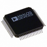
ADUC7128BSTZ126-RL Analog Devices Inc, ADUC7128BSTZ126-RL Datasheet - Page 68

ADUC7128BSTZ126-RL
Manufacturer Part Number
ADUC7128BSTZ126-RL
Description
IC DAS MCU ARM7 ADC/DDS 64-LQFP
Manufacturer
Analog Devices Inc
Series
MicroConverter® ADuC7xxxr
Datasheet
1.EVAL-ADUC7128QSPZ.pdf
(92 pages)
Specifications of ADUC7128BSTZ126-RL
Core Size
16/32-Bit
Program Memory Size
126KB (126K x 8)
Core Processor
ARM7
Speed
41.78MHz
Connectivity
I²C, SPI, UART/USART
Peripherals
PLA, POR, PWM, PSM, Temp Sensor, WDT
Number Of I /o
28
Program Memory Type
FLASH
Ram Size
8K x 8
Voltage - Supply (vcc/vdd)
3 V ~ 3.6 V
Data Converters
A/D 10x12b; D/A 1x10b
Oscillator Type
Internal
Operating Temperature
-40°C ~ 125°C
Package / Case
64-LQFP
Controller Family/series
(ARM7) ADUC
No. Of I/o's
40
Cpu Speed
41.78MHz
No. Of Timers
5
Digital Ic Case Style
LQFP
Embedded Interface Type
I2C, SPI, UART
Rohs Compliant
Yes
Lead Free Status / RoHS Status
Lead free / RoHS Compliant
For Use With
EVAL-ADUC7128QSPZ - KIT DEV FOR ADUC7128
Eeprom Size
-
Lead Free Status / RoHS Status
Lead free / RoHS Compliant, Lead free / RoHS Compliant
Other names
ADUC7128BSTZ126-RLTR
Available stocks
Company
Part Number
Manufacturer
Quantity
Price
Company:
Part Number:
ADUC7128BSTZ126-RL
Manufacturer:
Analog Devices Inc
Quantity:
10 000
ADuC7128/ADuC7129
Bit
7
6
5
4
3
2
1
0
I2CxDIV Register
Name
I2C0DIV
I2C1DIV
I2CxDIV are the clock divider registers.
I2CxIDx Register
Name
I2C0ID0
I2C0ID1
I2C0ID2
I2C0ID3
I2C1ID0
I2C1ID1
I2C1ID2
I2C1ID3
I2CxID0, I2CxID1, I2CxID2, and I2CxID3 are slave address
device ID registers of I2Cx.
Description
Master Serial Clock Enable Bit.
Loop-Back Enable Bit.
Start Back-Off Disable Bit.
Hardware General Call Enable. When this bit and Bit 3 are set, and have received a general call (Address 0x00) and a data byte, the
device checks the contents of the I2C0ALT against the receive register. If the contents match, the device has received a hardware
general call. This is used if a device needs urgent attention from a master device without knowing which master it needs to turn to.
This is a “to whom it may concern” call. The ADuC7128/ADuC7129 watch for these addresses. The device that requires attention
embeds its own address into the message. All masters listen and the one that can handle the device contacts its slave and acts
appropriately. The LSB of the I2C0ALT register should always be written to a 1, as per the I
General Call Enable Bit.
Reserved.
Master Enable Bit.
Slave Enable Bit.
Address
0xFFFF0830
0xFFFF0930
0xFFFF0838
0xFFFF083C
0xFFFF0840
0xFFFF0844
0xFFFF0938
0xFFFF093C
0xFFFF0940
0xFFFF0944
Address
Set by user to enable generation of the serial clock in master mode.
Cleared by user to disable serial clock in master mode.
Set by user to internally connect the transition to the reception to test user software.
Cleared by user to operate in normal mode.
Set by user in multimaster mode. If losing arbitration, the master immediately tries to retransmit.
Cleared by user to enable start back-off. After losing arbitration, the master waits before trying to retransmit.
Set this bit to enable the slave device to acknowledge an I
bit. If it receives a 0x06 (reset and write programmable part of slave address by hardware) as the data byte, the I
the I
sets on any general call. The user must take corrective action by setting up the I
(write programmable part of slave address by hardware) as the data byte, the general call interrupt status bit sets on any general
call. The user must take corrective action by reprogramming the device address.
Set by user to enable the master I
Cleared by user to disable the master I
Set by user to enable the slave I
I2C0ID2, and I2C0ID3. If the device address is recognized, the part participates in the slave transfer sequence.
Cleared by user to disable the slave I
2
C January 2000 specification. This command can be used to reset an entire I
Default Value
0x1F1F
0x1F1F
Default Value
0x00
0x00
0x00
0x00
0x00
0x00
0x00
0x00
2
C channel. A slave transfer sequence is monitored for the device address in I2C0ID0, I2C0ID1,
2
C channel.
2
C channel.
2
C channel.
Access
R/W
R/W
R/W
R/W
R/W
R/W
R/W
R/W
Access
R/W
R/W
Rev. 0 | Page 68 of 92
2
C general call, Address 0x00 (write). The device then recognizes a data
I2CxSSC Register
Name
I2C0SSC
I2C1SSC
I2CxSSC is an 8-bit start/stop generation counter. It holds off
SDA low for start and stop conditions.
Address
0xFFFF0848
0xFFFF0948
2
C interface after a reset. If it receives a 0x04
2
C system. The general call interrupt status bit
2
C January 2000 specification.
Default Value
0x01
0x01
2
C interface resets as per
Access
R/W
R/W


