UPSD3422EV-40U6 STMicroelectronics, UPSD3422EV-40U6 Datasheet - Page 213
UPSD3422EV-40U6
Manufacturer Part Number
UPSD3422EV-40U6
Description
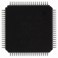
MCU 8BIT 8032 64KB FLASH 80TQFP
Manufacturer
STMicroelectronics
Series
µPSDr
Datasheet
1.UPSD3422EV-40U6.pdf
(300 pages)
Specifications of UPSD3422EV-40U6
Core Processor
8032
Core Size
8-Bit
Speed
40MHz
Connectivity
I²C, IrDA, SPI, UART/USART, USB
Peripherals
LVD, POR, PWM, WDT
Number Of I /o
46
Program Memory Size
80KB (80K x 8)
Program Memory Type
FLASH
Ram Size
4K x 8
Voltage - Supply (vcc/vdd)
3 V ~ 3.6 V
Data Converters
A/D 8x10b
Oscillator Type
Internal
Operating Temperature
-40°C ~ 85°C
Package / Case
80-TQFP, 80-VQFP
For Use With
497-5577 - BOARD EVAL USB POWER SWITCH497-5518 - EVAL BOARD RFID READER
Lead Free Status / RoHS Status
Lead free / RoHS Compliant
Eeprom Size
-
Other names
497-4905
Available stocks
Company
Part Number
Manufacturer
Quantity
Price
Company:

Part Number:
UPSD3422EV-40U6
Manufacturer:
STMicroelectronics
Quantity:
240
Company:
Part Number:
UPSD3422EV-40U6
Manufacturer:
STMicroelectronics
Quantity:
10 000


UPSD3422, UPSD3433, UPSD3434, UPSD3454
28.5.11
Data polling
Polling on the Data Polling Flag Bit (DQ7) is a method of checking whether a program or
erase operation is in progress or has completed.
algorithm.
When the 8032 issues a program instruction sequence, the embedded algorithm within the
Flash memory array begins. The 8032 then reads the location of the byte to be programmed
in Flash memory to check status. The Data Polling Flag Bit (DQ7) of this location becomes
the compliment of Bit D7 of the original data byte to be programmed. The 8032 continues to
poll this location, comparing the Data Polling Flag Bit (DQ7) and monitoring the Error Flag
Bit (DQ5). When the Data Polling Flag Bit (DQ7) matches Bit D7 of the original data, then
the embedded algorithm is complete. If the Error Flag Bit (DQ5) is '1,' the 8032 should test
the Data Polling Flag Bit (DQ7) again since the Data Polling Flag Bit (DQ7) may have
changed simultaneously with the Error Flag Bit (DQ5) (see
The Error Flag Bit (DQ5) is set if either an internal time-out occurred while the embedded
algorithm attempted to program the byte (indicating a bad Flash cell) or if the 8032
attempted to program bit to logic ’1’ when that bit was already programmed to logic ’0’ (must
erase to achieve logic ’1’).
It is suggested (as with all Flash memories) to read the location again after the embedded
programming algorithm has completed, to compare the byte that was written to the Flash
memory with the byte that was intended to be written.
When using the Data Polling method during an erase operation,
However, the Data Polling Flag Bit (DQ7) is '0' until the erase operation is complete. A ’1’ on
the Error Flag Bit (DQ5) indicates a time-out condition on the Erase cycle, a ’0’ indicates no
error. The 8032 can read any location within the sector being erased to get the Data Polling
Flag Bit (DQ7) and the Error Flag Bit (DQ5).
Figure 71
Figure
shows the Data Polling
Figure 71
71).
still applies.
PSD module
213/300
Related parts for UPSD3422EV-40U6
Image
Part Number
Description
Manufacturer
Datasheet
Request
R

Part Number:
Description:
Fast Turbo 8032 MCU with USB and Programmable Logic
Manufacturer:
STMICROELECTRONICS [STMicroelectronics]
Datasheet:

Part Number:
Description:
MCU 8BIT 8032 64KB FLASH 80TQFP
Manufacturer:
STMicroelectronics
Datasheet:

Part Number:
Description:
MCU 8BIT 8032 64KB FLASH 52TQFP
Manufacturer:
STMicroelectronics
Datasheet:
Part Number:
Description:
STMicroelectronics [RIPPLE-CARRY BINARY COUNTER/DIVIDERS]
Manufacturer:
STMicroelectronics
Datasheet:
Part Number:
Description:
STMicroelectronics [LIQUID-CRYSTAL DISPLAY DRIVERS]
Manufacturer:
STMicroelectronics
Datasheet:

Part Number:
Description:
BOARD EVAL FOR MEMS SENSORS
Manufacturer:
STMicroelectronics
Datasheet:
Part Number:
Description:
NPN TRANSISTOR POWER MODULE
Manufacturer:
STMicroelectronics
Datasheet:
Part Number:
Description:
TURBOSWITCH ULTRA-FAST HIGH VOLTAGE DIODE
Manufacturer:
STMicroelectronics
Datasheet:
Part Number:
Description:
Manufacturer:
STMicroelectronics
Datasheet:
Part Number:
Description:
DIODE / SCR MODULE
Manufacturer:
STMicroelectronics
Datasheet:
Part Number:
Description:
DIODE / SCR MODULE
Manufacturer:
STMicroelectronics
Datasheet:
Part Number:
Description:
Search -----> STE16N100
Manufacturer:
STMicroelectronics
Datasheet: