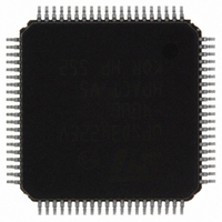
UPSD3422EV-40U6 STMicroelectronics, UPSD3422EV-40U6 Datasheet - Page 215

UPSD3422EV-40U6
Manufacturer Part Number
UPSD3422EV-40U6
Description
MCU 8BIT 8032 64KB FLASH 80TQFP
Manufacturer
STMicroelectronics
Series
µPSDr
Datasheet
1.UPSD3422EV-40U6.pdf
(300 pages)
Specifications of UPSD3422EV-40U6
Core Processor
8032
Core Size
8-Bit
Speed
40MHz
Connectivity
I²C, IrDA, SPI, UART/USART, USB
Peripherals
LVD, POR, PWM, WDT
Number Of I /o
46
Program Memory Size
80KB (80K x 8)
Program Memory Type
FLASH
Ram Size
4K x 8
Voltage - Supply (vcc/vdd)
3 V ~ 3.6 V
Data Converters
A/D 8x10b
Oscillator Type
Internal
Operating Temperature
-40°C ~ 85°C
Package / Case
80-TQFP, 80-VQFP
For Use With
497-5577 - BOARD EVAL USB POWER SWITCH497-5518 - EVAL BOARD RFID READER
Lead Free Status / RoHS Status
Lead free / RoHS Compliant
Eeprom Size
-
Other names
497-4905
Available stocks
Company
Part Number
Manufacturer
Quantity
Price
Company:
Part Number:
UPSD3422EV-40U6
Manufacturer:
STMicroelectronics
Quantity:
240
Company:
Part Number:
UPSD3422EV-40U6
Manufacturer:
STMicroelectronics
Quantity:
10 000
- Current page: 215 of 300
- Download datasheet (3Mb)
UPSD3422, UPSD3433, UPSD3434, UPSD3454
28.5.13
28.5.14
Bit (DQ5) indicates a time-out condition on the Erase cycle, a ’0’ indicates no error. The
8032 can read any location within the sector being erased to get the Toggle Flag Bit (DQ6)
and the Error Flag Bit (DQ5).
PSDsoft Express generates ANSI C code functions the user may use to implement these
Data Toggling algorithms.
Figure 72. Data toggle flowchart
Ready/Busy (PC3)
This signal can be used to output the Ready/Busy status of a program or erase operation on
either Flash memory. The output on the Ready/Busy pin is a ’0’ (Busy) when either Flash
memory array is being written, or when either Flash memory array is being erased. The
output is a ’1’ (Ready) when no program or erase operation is in progress. To activate this
function on this pin, the user must select the “Ready/Busy” selection in PSDsoft Express
when configuring pin PC3. This pin may be polled by the 8032 or used as a 8032 interrupt to
indicate when an erase or program operation is complete (requires routing the signal on PC
board from PC3 back into a pin on the MCU module). This signal is also available internally
on the PSD module as an input to both PLDs (without routing a signal externally on PC
board) and its signal name is “rd_bsy”. The Ready/Busy output can be probed during lab
development to check the timing of Flash memory programming in the system at run-time.
Bypassed unlock sequence
The Bypass Unlock mode allows the 8032 to program bytes in the Flash memories faster
than using the standard Flash program instruction sequences because the typical AAh, 55h
unlock bus cycles are bypassed for each byte that is programmed. Bypassing the unlock
NO
DQ5 & DQ6
READ DQ6
TOGGLE
TOGGLE
START
READ
DQ6
DQ5
DQ6
FAIL
= 1
=
=
YES
YES
YES
NO
NO
PASS
AI01370B
PSD module
215/300
Related parts for UPSD3422EV-40U6
Image
Part Number
Description
Manufacturer
Datasheet
Request
R

Part Number:
Description:
Fast Turbo 8032 MCU with USB and Programmable Logic
Manufacturer:
STMICROELECTRONICS [STMicroelectronics]
Datasheet:

Part Number:
Description:
MCU 8BIT 8032 64KB FLASH 80TQFP
Manufacturer:
STMicroelectronics
Datasheet:

Part Number:
Description:
MCU 8BIT 8032 64KB FLASH 52TQFP
Manufacturer:
STMicroelectronics
Datasheet:

Part Number:
Description:
STMicroelectronics [RIPPLE-CARRY BINARY COUNTER/DIVIDERS]
Manufacturer:
STMicroelectronics
Datasheet:

Part Number:
Description:
STMicroelectronics [LIQUID-CRYSTAL DISPLAY DRIVERS]
Manufacturer:
STMicroelectronics
Datasheet:

Part Number:
Description:
BOARD EVAL FOR MEMS SENSORS
Manufacturer:
STMicroelectronics
Datasheet:

Part Number:
Description:
NPN TRANSISTOR POWER MODULE
Manufacturer:
STMicroelectronics
Datasheet:

Part Number:
Description:
TURBOSWITCH ULTRA-FAST HIGH VOLTAGE DIODE
Manufacturer:
STMicroelectronics
Datasheet:

Part Number:
Description:
Manufacturer:
STMicroelectronics
Datasheet:

Part Number:
Description:
DIODE / SCR MODULE
Manufacturer:
STMicroelectronics
Datasheet:

Part Number:
Description:
DIODE / SCR MODULE
Manufacturer:
STMicroelectronics
Datasheet:

Part Number:
Description:
Search -----> STE16N100
Manufacturer:
STMicroelectronics
Datasheet:


