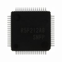
R5F212A8SNFP#U0 Renesas Electronics America, R5F212A8SNFP#U0 Datasheet - Page 502

R5F212A8SNFP#U0
Manufacturer Part Number
R5F212A8SNFP#U0
Description
IC R8C/2A MCU FLASH 64LQFP
Manufacturer
Renesas Electronics America
Series
R8C/2x/2Ar
Specifications of R5F212A8SNFP#U0
Core Processor
R8C
Core Size
16/32-Bit
Speed
20MHz
Connectivity
I²C, LIN, SIO, SSU, UART/USART
Peripherals
POR, PWM, Voltage Detect, WDT
Number Of I /o
55
Program Memory Size
64KB (64K x 8)
Program Memory Type
FLASH
Ram Size
3K x 8
Voltage - Supply (vcc/vdd)
2.2 V ~ 5.5 V
Data Converters
A/D 12x10b; D/A 2x8b
Oscillator Type
Internal
Operating Temperature
-20°C ~ 85°C
Package / Case
64-LQFP
For Use With
R0K5212D8S001BE - KIT STARTER FOR R8C/2DR0K5212D8S000BE - KIT DEV FOR R8C/2D
Lead Free Status / RoHS Status
Lead free / RoHS Compliant
Eeprom Size
-
Available stocks
Company
Part Number
Manufacturer
Quantity
Price
- Current page: 502 of 611
- Download datasheet (7Mb)
R8C/2A Group, R8C/2B Group
Rev.2.00
REJ09B0324-0200
18.2
Table 18.3
Function
Start conditions
Stop condition
Interrupt request generation
timing
Input pin
Reading of result of A/D
converter
In repeat mode, the input voltage of one selected pin is A/D converted repeatedly.
Table 18.3 lists the Repeat Mode 0 Specifications. Figure 18.7 shows the ADCON0 Register in Repeat Mode 0 and
Figure 18.8 shows the ADCON1 Register in Repeat Mode 0.
Repeat Mode 0
Nov 26, 2007
Item
Repeat Mode 0 Specifications
Page 480 of 580
The Input voltage of one pin selected by bits CH2 to CH0 and ADGSEL0 is
A/D converted repeatedly
• When the ADCAP bit is set to 0 (software trigger),
• When the ADCAP bit is set to 1 (starts in timer RD (complementary PWM
Set the ADST bit to 0
Not generated
Select one of AN0 to AN11
Read AD0 register
mode)), a compare match between registers TRD0 and TRDGRA0 or a
TRD1 underflow is generated while the ADST bit is set to 1
set the ADST bit to 1 (A/D conversion starts)
Specification
18. A/D Converter
Related parts for R5F212A8SNFP#U0
Image
Part Number
Description
Manufacturer
Datasheet
Request
R

Part Number:
Description:
KIT STARTER FOR M16C/29
Manufacturer:
Renesas Electronics America
Datasheet:

Part Number:
Description:
KIT STARTER FOR R8C/2D
Manufacturer:
Renesas Electronics America
Datasheet:

Part Number:
Description:
R0K33062P STARTER KIT
Manufacturer:
Renesas Electronics America
Datasheet:

Part Number:
Description:
KIT STARTER FOR R8C/23 E8A
Manufacturer:
Renesas Electronics America
Datasheet:

Part Number:
Description:
KIT STARTER FOR R8C/25
Manufacturer:
Renesas Electronics America
Datasheet:

Part Number:
Description:
KIT STARTER H8S2456 SHARPE DSPLY
Manufacturer:
Renesas Electronics America
Datasheet:

Part Number:
Description:
KIT STARTER FOR R8C38C
Manufacturer:
Renesas Electronics America
Datasheet:

Part Number:
Description:
KIT STARTER FOR R8C35C
Manufacturer:
Renesas Electronics America
Datasheet:

Part Number:
Description:
KIT STARTER FOR R8CL3AC+LCD APPS
Manufacturer:
Renesas Electronics America
Datasheet:

Part Number:
Description:
KIT STARTER FOR RX610
Manufacturer:
Renesas Electronics America
Datasheet:

Part Number:
Description:
KIT STARTER FOR R32C/118
Manufacturer:
Renesas Electronics America
Datasheet:

Part Number:
Description:
KIT DEV RSK-R8C/26-29
Manufacturer:
Renesas Electronics America
Datasheet:

Part Number:
Description:
KIT STARTER FOR SH7124
Manufacturer:
Renesas Electronics America
Datasheet:

Part Number:
Description:
KIT STARTER FOR H8SX/1622
Manufacturer:
Renesas Electronics America
Datasheet:

Part Number:
Description:
KIT DEV FOR SH7203
Manufacturer:
Renesas Electronics America
Datasheet:


