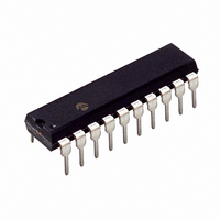
PIC16C770-I/P Microchip Technology, PIC16C770-I/P Datasheet - Page 105

PIC16C770-I/P
Manufacturer Part Number
PIC16C770-I/P
Description
IC MCU CMOS A/D 2K 20MHZ 20-DIP
Manufacturer
Microchip Technology
Series
PIC® 16Cr
Datasheets
1.PIC16C770-ISO.pdf
(220 pages)
2.PIC16C770-ISO.pdf
(6 pages)
3.PIC16C770-ISO.pdf
(8 pages)
Specifications of PIC16C770-I/P
Core Size
8-Bit
Program Memory Size
3.5KB (2K x 14)
Oscillator Type
Internal
Core Processor
PIC
Speed
20MHz
Connectivity
I²C, SPI
Peripherals
Brown-out Detect/Reset, POR, PWM, WDT
Number Of I /o
15
Program Memory Type
OTP
Ram Size
256 x 8
Voltage - Supply (vcc/vdd)
4 V ~ 5.5 V
Data Converters
A/D 6x12b
Operating Temperature
-40°C ~ 85°C
Package / Case
20-DIP (0.300", 7.62mm)
Controller Family/series
PIC16C
No. Of I/o's
16
Ram Memory Size
256Byte
Cpu Speed
20MHz
No. Of Timers
3
No. Of
RoHS Compliant
Core
PIC
Processor Series
PIC16C
Data Bus Width
8 bit
Maximum Clock Frequency
20 MHz
Data Ram Size
256 B
Data Rom Size
256 B
On-chip Adc
6 bit
Number Of Programmable I/os
16
Number Of Timers
3 bit
Operating Supply Voltage
2.5 V to 5.5 V
Mounting Style
Through Hole
Height
3.3 mm
Interface Type
I2C, SPI, SSP
Length
26.16 mm
Maximum Operating Temperature
+ 85 C
Minimum Operating Temperature
- 40 C
Supply Voltage (max)
5.5 V
Supply Voltage (min)
4 V
Width
6.35 mm
Lead Free Status / RoHS Status
Lead free / RoHS Compliant
For Use With
DVA16XP200 - ADAPTER ICE 20DIP/SOIC/SSOPAC164028 - MODULE SKT PROMATEII 20SOIC/DIP
Eeprom Size
-
Lead Free Status / Rohs Status
Details
Other names
PIC16C770I/P
- Current page: 105 of 220
- Download datasheet (4Mb)
10.1
The bandgap module generates a stable voltage refer-
ence of over a range of temperatures and device sup-
ply voltages. This module is enabled anytime any of the
following are enabled:
• Brown-out Reset
• Low-voltage Detect
• Either of the internal analog references (VRH,
Whenever the above are all disabled, the bandgap
module is disabled and draws no current.
10.2
The bandgap output voltage is used to generate two
stable references for the A/D converter module. These
references are enabled in software to provide the user
with the means to turn them on and off in order to min-
imize current consumption. Each reference can be indi-
vidually enabled.
The VRH reference is enabled with control bit VRHEN
(REFCON<7>). When this bit is set, the gain amplifier
is enabled. After a specified start-up time a stable ref-
erence of 4.096V nominal is generated and can be
used by the A/D converter as a reference input.
FIGURE 10-1: BLOCK DIAGRAM OF LVD AND VOLTAGE REFERENCE CIRCUIT
VRL)
2002 Microchip Technology Inc.
RA1/AN1/LVDIN
Bandgap Voltage Reference
Internal V
LVDEN
REF
V
DD
for A/D Converter
BODEN
BGAP
LVDEN
The VRL reference is enabled by setting control bit
VRLEN (REFCON<6>). When this bit is set, the gain
amplifier is enabled. After a specified start-up time a
stable reference of 2.048V nominal is generated and
can be used by the A/D converter as a reference input.
Each voltage reference is available for external use via
VRL and VRH pins.
Each reference, if enabled, can be output on an exter-
nal pin by setting the VRHOEN (high reference output
enable) or VRLOEN (low reference output enable) con-
trol bit. If the reference is not enabled, the VRHOEN
and VRLOEN bits will have no effect on the corre-
sponding pin. The device specific pin can then be used
as general purpose I/O.
Note:
PIC16C717/770/771
LVDCON
If VRH or VRL is enabled and the other ref-
erence (VRL or VRH), the BOR, and the
LVD modules are not enabled, the band-
gap will require a start-up time before the
bandgap reference is stable. Before using
the internal VRH or VRL reference, ensure
that the bandgap reference voltage is sta-
ble by monitoring the BGST bit in the LVD-
CON register. The voltage references will
not be reliable until the bandgap is stable
as shown by BGST being set.
VRHEN + VRLEN
generates
LVDIF
REFCON
VRL
VRH
DS41120B-page 103
Related parts for PIC16C770-I/P
Image
Part Number
Description
Manufacturer
Datasheet
Request
R

Part Number:
Description:
IC MCU OTP 8KX14 A/D PWM 44PLCC
Manufacturer:
Microchip Technology
Datasheet:

Part Number:
Description:
IC MCU OTP 8KX14 A/D PWM 44PLCC
Manufacturer:
Microchip Technology
Datasheet:

Part Number:
Description:
IC MCU OTP 8KX14 A/D PWM 44TQFP
Manufacturer:
Microchip Technology
Datasheet:

Part Number:
Description:
IC MCU OTP 8KX14 A/D PWM 44-MQFP
Manufacturer:
Microchip Technology
Datasheet:

Part Number:
Description:
IC MCU OTP 8KX14 A/D PWM 40DIP
Manufacturer:
Microchip Technology
Datasheet:

Part Number:
Description:
IC MCU OTP 8KX14 A/D PWM 44PLCC
Manufacturer:
Microchip Technology
Datasheet:

Part Number:
Description:
IC MCU OTP 8KX14 A/D PWM 40DIP
Manufacturer:
Microchip Technology
Datasheet:

Part Number:
Description:
IC MCU OTP 8KX14 A/D PWM 40DIP
Manufacturer:
Microchip Technology
Datasheet:

Part Number:
Description:
IC MCU OTP 8KX14 A/D PWM 40DIP
Manufacturer:
Microchip Technology
Datasheet:

Part Number:
Description:
IC MCU OTP 8KX14 A/D PWM 44PLCC
Manufacturer:
Microchip Technology
Datasheet:

Part Number:
Description:
IC MCU OTP 8KX14 A/D PWM 44PLCC
Manufacturer:
Microchip Technology
Datasheet:

Part Number:
Description:
IC MCU OTP 8KX14 A/D PWM 44-MQFP
Manufacturer:
Microchip Technology
Datasheet:

Part Number:
Description:
IC MCU OTP 8KX14 A/D PWM 40DIP
Manufacturer:
Microchip Technology
Datasheet:

Part Number:
Description:
IC MCU OTP 8KX14 A/D PWM 44-MQFP
Manufacturer:
Microchip Technology
Datasheet:

Part Number:
Description:
IC MCU OTP 8KX14 A/D PWM 40DIP
Manufacturer:
Microchip Technology
Datasheet:


