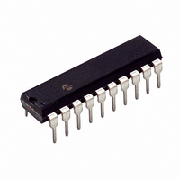
PIC16C770-I/P Microchip Technology, PIC16C770-I/P Datasheet - Page 66

PIC16C770-I/P
Manufacturer Part Number
PIC16C770-I/P
Description
IC MCU CMOS A/D 2K 20MHZ 20-DIP
Manufacturer
Microchip Technology
Series
PIC® 16Cr
Datasheets
1.PIC16C770-ISO.pdf
(220 pages)
2.PIC16C770-ISO.pdf
(6 pages)
3.PIC16C770-ISO.pdf
(8 pages)
Specifications of PIC16C770-I/P
Core Size
8-Bit
Program Memory Size
3.5KB (2K x 14)
Oscillator Type
Internal
Core Processor
PIC
Speed
20MHz
Connectivity
I²C, SPI
Peripherals
Brown-out Detect/Reset, POR, PWM, WDT
Number Of I /o
15
Program Memory Type
OTP
Ram Size
256 x 8
Voltage - Supply (vcc/vdd)
4 V ~ 5.5 V
Data Converters
A/D 6x12b
Operating Temperature
-40°C ~ 85°C
Package / Case
20-DIP (0.300", 7.62mm)
Controller Family/series
PIC16C
No. Of I/o's
16
Ram Memory Size
256Byte
Cpu Speed
20MHz
No. Of Timers
3
No. Of
RoHS Compliant
Core
PIC
Processor Series
PIC16C
Data Bus Width
8 bit
Maximum Clock Frequency
20 MHz
Data Ram Size
256 B
Data Rom Size
256 B
On-chip Adc
6 bit
Number Of Programmable I/os
16
Number Of Timers
3 bit
Operating Supply Voltage
2.5 V to 5.5 V
Mounting Style
Through Hole
Height
3.3 mm
Interface Type
I2C, SPI, SSP
Length
26.16 mm
Maximum Operating Temperature
+ 85 C
Minimum Operating Temperature
- 40 C
Supply Voltage (max)
5.5 V
Supply Voltage (min)
4 V
Width
6.35 mm
Lead Free Status / RoHS Status
Lead free / RoHS Compliant
For Use With
DVA16XP200 - ADAPTER ICE 20DIP/SOIC/SSOPAC164028 - MODULE SKT PROMATEII 20SOIC/DIP
Eeprom Size
-
Lead Free Status / Rohs Status
Details
Other names
PIC16C770I/P
PIC16C717/770/771
8.3.7
When the ECCP module is used in the PWM mode, the
application hardware must use the proper external pull-
up and/or pull-down resistors on the PWM output pins.
When the microcontroller powers up, all of the I/O pins
are in the high-impedance state. The external pull-up
and pull-down resistors must keep the power switch
devices in the off state until the microcontroller drives
the I/O pins with the proper signal levels, or activates
the PWM output(s).
8.3.8
Prior to enabling the PWM outputs, the P1A, P1B, P1C
and P1D latches may not be in the proper states.
Enabling the TRISB bits for output at the same time
with the CCP module may cause damage to the power
switch devices. The CCP1 module must be enabled in
the proper Output mode with the TRISB bits enabled as
inputs. Once the CCP1 completes a full PWM cycle,
the P1A, P1B, P1C and P1D output latches are prop-
erly initialized. At this time, the TRISB bits can be
enabled for outputs to start driving the power switch
devices. The completion of a full PWM cycle is indi-
cated by the TMR2IF bit going from a ’0’ to a ’1’.
TABLE 8-3:
DS41120B-page 64
0Bh, 8Bh,
10Bh, 18Bh
0Ch
8Ch
86h, 186h
11h
92h
12h
15h
17h
97h
Legend:
Address
INTCON
PIR1
PIE1
TRISB
TMR2
PR2
T2CON
CCPR1L
CCP1CON PWM1M1
P1DEL
x = unknown, u = unchanged, - = unimplemented read as '0'. Shaded cells are not used by ECCP module in PWM mode.
SYSTEM IMPLEMENTATION
START-UP CONSIDERATIONS
Name
REGISTERS ASSOCIATED WITH PWM
PORTB Data Direction Register
Timer2 register
Timer2 period register
Capture/Compare/PWM register1 (LSB)
PWM1 Delay value
Bit 7
GIE
—
—
—
TOUTPS3 TOUTPS2 TOUTPS1 TOUTPS0
PWM1M0
ADIE
Bit 6
PEIE
ADIF
DC1B1
Bit 5
T0IE
—
—
DC1B0
INTE
Bit 4
—
—
CCP1M3
SSPIF
SSPIE
RBIE
Bit 3
8.3.9
The following steps should be taken when configuring
the ECCP module for PWM operation:
1.
2.
3.
Configure the PWM module:
a)
b)
c)
d)
e)
Configure and start TMR2:
a)
b)
c)
Enable PWM outputs after a new cycle has
started:
a)
b)
TMR2ON
CCP1M2
CCP1IE
CCP1IF
Bit 2
T0IF
Disable the CCP1/P1A, P1B, P1C and/or
P1D outputs by setting the respective
TRISB bits.
Set the PWM period by loading the PR2
register.
Set the PWM duty cycle by loading the
CCPR1L register and CCP1CON<5:4>
bits.
Configure the ECCP module for the desired
PWM operation by loading the CCP1CON
register. With the CCP1M<3:0> bits select
the active high/low levels for each PWM
output. With the PWM1M<1:0> bits select
one of the available Output modes: Single,
Half-Bridge, Full-Bridge, Forward or Full-
Bridge Reverse.
For Half-Bridge Output mode, set the dead-
band delay by loading the P1DEL register.
Clear the TMR2 interrupt flag bit by clearing
the TMR2IF bit in the PIR1 register.
Set the TMR2 prescale value by loading the
T2CKPS<1:0> bits in the T2CON register.
Enable Timer2 by setting the TMR2ON bit
in the T2CON register.
Wait until TMR2 overflows (TMR2IF bit
becomes a ’1’). The new PWM cycle begins
here.
Enable the CCP1/P1A, P1B, P1C and/or
P1D pin outputs by clearing the respective
TRISB bits.
SET UP FOR PWM OPERATION
T2CKPS1
CCP1M1
TMR2IE
TMR2IF
Bit 1
INTF
T2CKPS0 -000 0000 -000 0000
CCP1M0
TMR1IF
TMR1IE
2002 Microchip Technology Inc.
RBIF
Bit 0
0000 000x 0000 000u
-0-- 0000 -0-- 0000
-0-- 0000 -0-- 0000
1111 1111 1111 1111
0000 0000 0000 0000
1111 1111 1111 1111
xxxx xxxx uuuu uuuu
0000 0000 0000 0000
0000 0000 0000 0000
Value on
POR,
BOR
Value on
RESETS
all other


