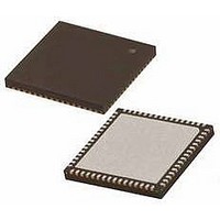
PIC18F65K22-I/MRRSL Microchip Technology, PIC18F65K22-I/MRRSL Datasheet - Page 253

PIC18F65K22-I/MRRSL
Manufacturer Part Number
PIC18F65K22-I/MRRSL
Description
MCU PIC 32K FLASH MEM XLP 64QFN
Manufacturer
Microchip Technology
Series
PIC® XLP™ 18Fr
Datasheets
1.PIC16F722-ISS.pdf
(8 pages)
2.PIC18F65K22T-IPTRSL.pdf
(548 pages)
3.PIC18F65K22T-IPTRSL.pdf
(10 pages)
Specifications of PIC18F65K22-I/MRRSL
Core Size
8-Bit
Program Memory Size
32KB (16K x 16)
Core Processor
PIC
Speed
64MHz
Connectivity
I²C, LIN, SPI, UART/USART
Peripherals
Brown-out Detect/Reset, LVD, POR, PWM, WDT
Number Of I /o
53
Program Memory Type
FLASH
Eeprom Size
1K x 8
Ram Size
2K x 8
Voltage - Supply (vcc/vdd)
1.8 V ~ 5.5 V
Data Converters
A/D 16x12b
Oscillator Type
Internal
Operating Temperature
-40°C ~ 85°C
Package / Case
64-VFQFN, Exposed Pad
Controller Family/series
PIC18
No. Of I/o's
53
Eeprom Memory Size
1KB
Ram Memory Size
2KB
Cpu Speed
64MHz
No. Of Timers
8
Processor Series
PIC18F
Core
PIC
Data Bus Width
8 bit
Data Ram Size
2 KB
Interface Type
I2C, SPI
Maximum Clock Frequency
64 MHz
Number Of Programmable I/os
53
Number Of Timers
8
Operating Supply Voltage
1.8 V to 5.5 V
Maximum Operating Temperature
+ 125 C
Mounting Style
SMD/SMT
3rd Party Development Tools
52715-96, 52716-328, 52717-734, 52712-325, EWPIC18
Minimum Operating Temperature
- 40 C
On-chip Adc
12 bit, 16 Channel
Lead Free Status / RoHS Status
Lead free / RoHS Compliant
Lead Free Status / RoHS Status
Lead free / RoHS Compliant
- PIC16F722-ISS PDF datasheet
- PIC18F65K22T-IPTRSL PDF datasheet #2
- PIC18F65K22T-IPTRSL PDF datasheet #3
- Current page: 253 of 548
- Download datasheet (5Mb)
19.4
In Pulse-Width Modulation (PWM) mode, the CCP4 pin
produces up to a 10-bit resolution PWM output. Since
the CCP4 pin is multiplexed with a PORTC or PORTE
data latch, the appropriate TRIS bit must be cleared to
make the CCP4 pin an output.
Figure 19-3 shows a simplified block diagram of the
ECCP1 module in PWM mode.
For a step-by-step procedure on how to set up the CCP
module for PWM operation, see Section 19.4.3
“Setup for PWM Operation”.
FIGURE 19-3:
2010 Microchip Technology Inc.
Note 1:
2:
Note:
CCPR4H (Slave)
Duty Cycle Registers
Comparator
CCPR4L
TMR2
PR2
Comparator
PWM Mode
The 8-bit TMR2 value is concatenated with the 2-bit
internal Q clock, or 2 bits of the prescaler, to create
the 10-bit time base.
CCP4 and its appropriate timers are used as an
example. For details on all of the CCP modules and
their timer assignments, see Table 19-2 and
Table 19-3.
Clearing the CCP4CON register will force
the RC1 or RE7 output latch (depending
on device configuration) to the default low
level. This is not the PORTC or PORTE
I/O data latch.
(Note 1)
Clear Timer,
ECCP1 Pin and
Latch D.C.
SIMPLIFIED PWM BLOCK
DIAGRAM
CCP4CON<5:4>
R
S
Q
TRISC<2>
RC2/ECCP1
Preliminary
PIC18F87K22 FAMILY
A PWM output (Figure 19-4) has a time base (period)
and a time that the output stays high (duty cycle). The
frequency of the PWM is the inverse of the period
(1/period).
FIGURE 19-4:
19.4.1
The PWM period is specified by writing to the PR2
register. The PWM period can be calculated using the
following formula:
EQUATION 19-1:
PWM frequency is defined as 1/[PWM period].
When TMR2 is equal to PR2, the following three events
occur on the next increment cycle:
• TMR2 is cleared
• The CCP4 pin is set
• The PWM duty cycle is latched from CCPR4L into
(An exception: If PWM duty cycle = 0%, the CCP4
pin will not be set)
CCPR4H
Note:
PWM Period = [(PR2) + 1] • 4 • T
TMR2 = PR2
Duty Cycle
PWM PERIOD
The Timer2 postscalers (see Section 15.0
“Timer2 Module”) are not used in the
determination of the PWM frequency. The
postscaler could be used to have a servo
update rate at a different frequency than
the PWM output.
Period
TMR2 = Duty Cycle
(TMR2 Prescale Value)
PWM OUTPUT
TMR2 = PR2
DS39960B-page 253
OSC
•
Related parts for PIC18F65K22-I/MRRSL
Image
Part Number
Description
Manufacturer
Datasheet
Request
R

Part Number:
Description:
MCU PIC 32K FLASH MEM XLP 64TQFP
Manufacturer:
Microchip Technology
Datasheet:

Part Number:
Description:
32kB Flash, 2kB RAM, 1kB EE, NanoWatt XLP, GP 64 QFN 9x9x0.9mm TUBE
Manufacturer:
Microchip Technology
Datasheet:

Part Number:
Description:
32kB Flash, 2kB RAM, 1kB EE, NanoWatt XLP, GP 64 TQFP 10x10x1mm TRAY
Manufacturer:
Microchip Technology
Datasheet:

Part Number:
Description:
32kB Flash, 2kB RAM, 1kB EE, NanoWatt XLP, GP 64 QFN 9x9x0.9mm TUBE
Manufacturer:
Microchip Technology
Datasheet:

Part Number:
Description:
32kB Flash, 2kB RAM, 1kB EE, NanoWatt XLP, GP 64 TQFP 10x10x1mm TRAY
Manufacturer:
Microchip Technology

Part Number:
Description:
Manufacturer:
Microchip Technology Inc.
Datasheet:

Part Number:
Description:
Manufacturer:
Microchip Technology Inc.
Datasheet:

Part Number:
Description:
Manufacturer:
Microchip Technology Inc.
Datasheet:

Part Number:
Description:
Manufacturer:
Microchip Technology Inc.
Datasheet:

Part Number:
Description:
Manufacturer:
Microchip Technology Inc.
Datasheet:

Part Number:
Description:
Manufacturer:
Microchip Technology Inc.
Datasheet:


