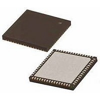
PIC18F65K22-I/MRRSL Microchip Technology, PIC18F65K22-I/MRRSL Datasheet - Page 473

PIC18F65K22-I/MRRSL
Manufacturer Part Number
PIC18F65K22-I/MRRSL
Description
MCU PIC 32K FLASH MEM XLP 64QFN
Manufacturer
Microchip Technology
Series
PIC® XLP™ 18Fr
Datasheets
1.PIC16F722-ISS.pdf
(8 pages)
2.PIC18F65K22T-IPTRSL.pdf
(548 pages)
3.PIC18F65K22T-IPTRSL.pdf
(10 pages)
Specifications of PIC18F65K22-I/MRRSL
Core Size
8-Bit
Program Memory Size
32KB (16K x 16)
Core Processor
PIC
Speed
64MHz
Connectivity
I²C, LIN, SPI, UART/USART
Peripherals
Brown-out Detect/Reset, LVD, POR, PWM, WDT
Number Of I /o
53
Program Memory Type
FLASH
Eeprom Size
1K x 8
Ram Size
2K x 8
Voltage - Supply (vcc/vdd)
1.8 V ~ 5.5 V
Data Converters
A/D 16x12b
Oscillator Type
Internal
Operating Temperature
-40°C ~ 85°C
Package / Case
64-VFQFN, Exposed Pad
Controller Family/series
PIC18
No. Of I/o's
53
Eeprom Memory Size
1KB
Ram Memory Size
2KB
Cpu Speed
64MHz
No. Of Timers
8
Processor Series
PIC18F
Core
PIC
Data Bus Width
8 bit
Data Ram Size
2 KB
Interface Type
I2C, SPI
Maximum Clock Frequency
64 MHz
Number Of Programmable I/os
53
Number Of Timers
8
Operating Supply Voltage
1.8 V to 5.5 V
Maximum Operating Temperature
+ 125 C
Mounting Style
SMD/SMT
3rd Party Development Tools
52715-96, 52716-328, 52717-734, 52712-325, EWPIC18
Minimum Operating Temperature
- 40 C
On-chip Adc
12 bit, 16 Channel
Lead Free Status / RoHS Status
Lead free / RoHS Compliant
Lead Free Status / RoHS Status
Lead free / RoHS Compliant
- PIC16F722-ISS PDF datasheet
- PIC18F65K22T-IPTRSL PDF datasheet #2
- PIC18F65K22T-IPTRSL PDF datasheet #3
- Current page: 473 of 548
- Download datasheet (5Mb)
CALLW
Syntax:
Operands:
Operation:
Status Affected:
Encoding:
Description
Words:
Cycles:
Example:
2010 Microchip Technology Inc.
Q Cycle Activity:
Before Instruction
After Instruction
operation
Decode
No
PC
PCLATH =
PCLATU =
W
PC
TOS
PCLATH =
PCLATU =
W
Q1
=
=
=
=
=
operation
Subroutine Call Using WREG
CALLW
None
(PC + 2) TOS,
(W) PCL,
(PCLATH) PCH,
(PCLATU) PCU
None
First, the return address (PC + 2) is
pushed onto the return stack. Next, the
contents of W are written to PCL; the
existing value is discarded. Then, the
contents of PCLATH and PCLATU are
latched into PCH and PCU,
respectively. The second cycle is
executed as a NOP instruction while the
new next instruction is fetched.
Unlike CALL , there is no option to
update W, STATUS or BSR.
1
2
HERE
WREG
Read
0000
No
Q2
address (HERE)
10h
00h
06h
001006h
address (HERE + 2)
10h
00h
06h
CALLW
0000
Push PC to
operation
stack
No
Q3
0001
operation
operation
No
No
Q4
0100
Preliminary
PIC18F87K22 FAMILY
MOVSF
Syntax:
Operands:
Operation:
Status Affected:
Encoding:
1st word (source)
2nd word (destin.)
Description:
Words:
Cycles:
Example:
Q Cycle Activity:
Before Instruction
After Instruction
Decode
Decode
FSR2
Contents
of 85h
REG2
FSR2
Contents
of 85h
REG2
Q1
source addr
No dummy
Determine
operation
Move Indexed to f
MOVSF [z
0 z
0 f
((FSR2) + z
None
The contents of the source register are
moved to destination register ‘f
actual address of the source register is
determined by adding the 7-bit literal
offset ‘z
of FSR2. The address of the destination
register is specified by the 12-bit literal
‘f
can be anywhere in the 4096-byte data
space (000h to FFFh).
The MOVSF instruction cannot use the
PCL, TOSU, TOSH or TOSL as the
destination register.
If the resultant source address points to
an Indirect Addressing register, the
value returned will be 00h.
2
2
MOVSF
d
read
’ in the second word. Both addresses
1110
1111
No
Q2
=
=
=
=
=
=
d
s
4095
127
s
’, in the first word, to the value
80h
33h
11h
80h
33h
33h
[05h], REG2
s
s
source addr
1011
ffff
], f
) f
Determine
operation
d
No
Q3
d
DS39960B-page 473
0zzz
ffff
source reg
register ‘f’
(dest)
Read
Write
d
Q4
zzzz
ffff
’. The
s
d
Related parts for PIC18F65K22-I/MRRSL
Image
Part Number
Description
Manufacturer
Datasheet
Request
R

Part Number:
Description:
MCU PIC 32K FLASH MEM XLP 64TQFP
Manufacturer:
Microchip Technology
Datasheet:

Part Number:
Description:
32kB Flash, 2kB RAM, 1kB EE, NanoWatt XLP, GP 64 QFN 9x9x0.9mm TUBE
Manufacturer:
Microchip Technology
Datasheet:

Part Number:
Description:
32kB Flash, 2kB RAM, 1kB EE, NanoWatt XLP, GP 64 TQFP 10x10x1mm TRAY
Manufacturer:
Microchip Technology
Datasheet:

Part Number:
Description:
32kB Flash, 2kB RAM, 1kB EE, NanoWatt XLP, GP 64 QFN 9x9x0.9mm TUBE
Manufacturer:
Microchip Technology
Datasheet:

Part Number:
Description:
32kB Flash, 2kB RAM, 1kB EE, NanoWatt XLP, GP 64 TQFP 10x10x1mm TRAY
Manufacturer:
Microchip Technology

Part Number:
Description:
Manufacturer:
Microchip Technology Inc.
Datasheet:

Part Number:
Description:
Manufacturer:
Microchip Technology Inc.
Datasheet:

Part Number:
Description:
Manufacturer:
Microchip Technology Inc.
Datasheet:

Part Number:
Description:
Manufacturer:
Microchip Technology Inc.
Datasheet:

Part Number:
Description:
Manufacturer:
Microchip Technology Inc.
Datasheet:

Part Number:
Description:
Manufacturer:
Microchip Technology Inc.
Datasheet:


