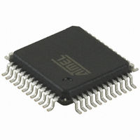
AT32UC3B164-AUT Atmel, AT32UC3B164-AUT Datasheet - Page 224

AT32UC3B164-AUT
Manufacturer Part Number
AT32UC3B164-AUT
Description
IC MCU AVR32 64KB FLASH 48-TQFP
Manufacturer
Atmel
Series
AVR®32 UC3r
Specifications of AT32UC3B164-AUT
Core Processor
AVR
Core Size
32-Bit
Speed
60MHz
Connectivity
I²C, IrDA, SPI, SSC, UART/USART, USB
Peripherals
Brown-out Detect/Reset, DMA, POR, PWM, WDT
Number Of I /o
28
Program Memory Size
64KB (64K x 8)
Program Memory Type
FLASH
Ram Size
16K x 8
Voltage - Supply (vcc/vdd)
1.65 V ~ 1.95 V
Data Converters
A/D 6x10b
Oscillator Type
Internal
Operating Temperature
-40°C ~ 85°C
Package / Case
48-TQFP, 48-VQFP
Controller Family/series
AT32UC3B
No. Of I/o's
28
Ram Memory Size
16KB
Cpu Speed
60MHz
No. Of Timers
1
Rohs Compliant
Yes
For Use With
ATSTK600-TQFP48 - STK600 SOCKET/ADAPTER 48-TQFPATAVRONEKIT - KIT AVR/AVR32 DEBUGGER/PROGRMMR770-1008 - ISP 4PORT ATMEL AVR32 MCU SPIATEVK1101 - KIT DEV/EVAL FOR AVR32 AT32UC3B
Lead Free Status / RoHS Status
Lead free / RoHS Compliant
Eeprom Size
-
Available stocks
Company
Part Number
Manufacturer
Quantity
Price
- Current page: 224 of 676
- Download datasheet (11Mb)
19.10 Master Mode
19.10.1
19.10.2
Figure 19-5. Master Mode Typical Application Block Diagram
19.10.3
19.10.4
32059I–06/2010
Definition
Application Block Diagram
Programming Master Mode
Master Transmitter Mode
Rp: Pull up value as given by the I²C Standard
Host with
Interface
TWI
The Master is the device which starts a transfer, generates a clock and stops it.
The following registers have to be programmed before entering Master mode:
1. DADR (+ IADRSZ + IADR if a 10 bit device is addressed): The device address is used to
2. CKDIV + CHDIV + CLDIV: Clock Waveform.
3. SVDIS: Disable the slave mode.
4. MSEN: Enable the master mode.
After the master initiates a Start condition when writing into the Transmit Holding Register, THR,
it sends a 7-bit slave address, configured in the Master Mode register (DADR in MMR), to notify
the slave device. The bit following the slave address indicates the transfer direction, 0 in this
case (MREAD = 0 in MMR).
The TWI transfers require the slave to acknowledge each received byte. During the acknowl-
edge clock pulse (9th pulse), the master releases the data line (HIGH), enabling the slave to pull
it down in order to generate the acknowledge. The master polls the data line during this clock
pulse and sets the NACK in the status register if the slave does not acknowledge the byte. As
with the other status bits, an interrupt can be generated if enabled in the interrupt enable register
(IER). If the slave acknowledges the byte, the data written in the THR, is then shifted in the inter-
nal shifter and transferred. When an acknowledge is detected, the TXRDY bit is set until a new
write in the THR. When no more data is written into the THR, the master generates a stop condi-
tion to end the transfer. The end of the complete transfer is marked by the TXCOMP bit set to
one. See
TXRDY is used as Transmit Ready for the Peripheral DMA Controller transmit channel.
TWD
TWCK
access slave devices in read or write mode.
Serial EEPROM
Atmel TWI
Slave 1
Figure
19-6,
Figure
I²C RTC
Slave 2
19-7, and
Controller
I²C LCD
Slave 3
Figure 19-8 on page
I²C Temp.
Slave 4
Sensor
225.
Rp
Rp
AT32UC3B
VDD
224
Related parts for AT32UC3B164-AUT
Image
Part Number
Description
Manufacturer
Datasheet
Request
R

Part Number:
Description:
DEV KIT FOR AVR/AVR32
Manufacturer:
Atmel
Datasheet:

Part Number:
Description:
INTERVAL AND WIPE/WASH WIPER CONTROL IC WITH DELAY
Manufacturer:
ATMEL Corporation
Datasheet:

Part Number:
Description:
Low-Voltage Voice-Switched IC for Hands-Free Operation
Manufacturer:
ATMEL Corporation
Datasheet:

Part Number:
Description:
MONOLITHIC INTEGRATED FEATUREPHONE CIRCUIT
Manufacturer:
ATMEL Corporation
Datasheet:

Part Number:
Description:
AM-FM Receiver IC U4255BM-M
Manufacturer:
ATMEL Corporation
Datasheet:

Part Number:
Description:
Monolithic Integrated Feature Phone Circuit
Manufacturer:
ATMEL Corporation
Datasheet:

Part Number:
Description:
Multistandard Video-IF and Quasi Parallel Sound Processing
Manufacturer:
ATMEL Corporation
Datasheet:

Part Number:
Description:
High-performance EE PLD
Manufacturer:
ATMEL Corporation
Datasheet:

Part Number:
Description:
8-bit Flash Microcontroller
Manufacturer:
ATMEL Corporation
Datasheet:

Part Number:
Description:
2-Wire Serial EEPROM
Manufacturer:
ATMEL Corporation
Datasheet:


