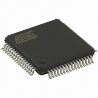
AT32UC3B0256-A2UR Atmel, AT32UC3B0256-A2UR Datasheet - Page 157

AT32UC3B0256-A2UR
Manufacturer Part Number
AT32UC3B0256-A2UR
Description
MCU AVR32 256K FLASH 64-TQFP
Manufacturer
Atmel
Series
AVR®32 UC3r
Datasheet
1.AT32UC3B1512-Z1UT.pdf
(692 pages)
Specifications of AT32UC3B0256-A2UR
Package / Case
64-TQFP, 64-VQFP
Voltage - Supply (vcc/vdd)
1.65 V ~ 1.95 V
Operating Temperature
-40°C ~ 85°C
Speed
60MHz
Number Of I /o
44
Core Processor
AVR
Program Memory Type
FLASH
Ram Size
32K x 8
Program Memory Size
256KB (256K x 8)
Data Converters
A/D 8x10b
Oscillator Type
Internal
Peripherals
Brown-out Detect/Reset, DMA, POR, PWM, WDT
Connectivity
I²C, IrDA, SPI, SSC, UART/USART, USB
Core Size
32-Bit
Package
64TQFP
Device Core
AVR32
Family Name
AT32
Maximum Speed
60 MHz
Operating Supply Voltage
1.8|3.3 V
Data Bus Width
32 Bit
Number Of Programmable I/os
44
Interface Type
I2S/SPI/TWI/USART/USB
On-chip Adc
8-chx10-bit
Number Of Timers
3
Lead Free Status / RoHS Status
Lead free / RoHS Compliant
Eeprom Size
-
Available stocks
Company
Part Number
Manufacturer
Quantity
Price
- Current page: 157 of 692
- Download datasheet (11Mb)
16.6
16.6.1
Table 16-1.
16.6.2
Table 16-2.
Note:
32059K–03/2011
0x00C
0x01C
0x02C
0x000
0x004
0x008
0x010
0x014
0x018
0x020
0x024
0x028
(0x000 - 0x03F)+m*0x040
User Interface
1. The reset values are device specific. Please refer to the Module Configuration section at the end of this chapter.
Offset
+ n*0x040
+ n*0x040
+ n*0x040
+ n*0x040
+ n*0x040
+ n*0x040
+ n*0x040
+ n*0x040
+ n*0x040
+ n*0x040
+ n*0x040
+ n*0x040
Address Range
0x000 - 0x03F
0x040 - 0x07F
Memory Map Overview
Channel Memory Map
PDCA Register Memory Map
PDCA Channel Configuration Registers
...
The channels are mapped as shown in
isters, shown in
Note:
Memory Address Reload Register
Transfer Counter Reload Register
Memory Address Register
Peripheral Select Register
Transfer Counter Register
Interrupt Disable Register
Interrupt Enable Register
Interrupt Status Register
Interrupt Mask Register
1. The reset values are device specific. Please refer to the Module Configuration section at the
Control Register
Status Register
Mode Register
end of this chapter.
Register
Table
16-2, where n is the channel number.
DMA channel m configuration registers
DMA channel 0 configuration registers
DMA channel 1 configuration registers
Table
Register Name
MARR
16-1. Each channel has a set of configuration reg-
TCRR
MAR
PSR
TCR
IMR
IER
IDR
ISR
MR
Contents
CR
SR
...
Read/Write
Read/Write
Read/Write
Read/Write
Read/Write
Read/Write
Write-only
Read-only
Write-only
Write-only
Read-only
Read-only
Access
AT32UC3B
0x00000000
0x00000000
0x00000000
0x00000000
0x00000000
0x00000000
0x00000000
0x00000000
0x00000000
0x00000000
0x00000000
Reset
-
(1)
157
Related parts for AT32UC3B0256-A2UR
Image
Part Number
Description
Manufacturer
Datasheet
Request
R

Part Number:
Description:
DEV KIT FOR AVR/AVR32
Manufacturer:
Atmel
Datasheet:

Part Number:
Description:
INTERVAL AND WIPE/WASH WIPER CONTROL IC WITH DELAY
Manufacturer:
ATMEL Corporation
Datasheet:

Part Number:
Description:
Low-Voltage Voice-Switched IC for Hands-Free Operation
Manufacturer:
ATMEL Corporation
Datasheet:

Part Number:
Description:
MONOLITHIC INTEGRATED FEATUREPHONE CIRCUIT
Manufacturer:
ATMEL Corporation
Datasheet:

Part Number:
Description:
AM-FM Receiver IC U4255BM-M
Manufacturer:
ATMEL Corporation
Datasheet:

Part Number:
Description:
Monolithic Integrated Feature Phone Circuit
Manufacturer:
ATMEL Corporation
Datasheet:

Part Number:
Description:
Multistandard Video-IF and Quasi Parallel Sound Processing
Manufacturer:
ATMEL Corporation
Datasheet:

Part Number:
Description:
High-performance EE PLD
Manufacturer:
ATMEL Corporation
Datasheet:

Part Number:
Description:
8-bit Flash Microcontroller
Manufacturer:
ATMEL Corporation
Datasheet:

Part Number:
Description:
2-Wire Serial EEPROM
Manufacturer:
ATMEL Corporation
Datasheet:


