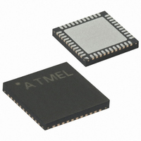
ATMEGA644V-10MU Atmel, ATMEGA644V-10MU Datasheet - Page 283

ATMEGA644V-10MU
Manufacturer Part Number
ATMEGA644V-10MU
Description
IC AVR MCU FLASH 64K 44-QFN
Manufacturer
Atmel
Series
AVR® ATmegar
Specifications of ATMEGA644V-10MU
Core Processor
AVR
Core Size
8-Bit
Speed
10MHz
Connectivity
I²C, SPI, UART/USART
Peripherals
Brown-out Detect/Reset, POR, PWM, WDT
Number Of I /o
32
Program Memory Size
64KB (32K x 16)
Program Memory Type
FLASH
Eeprom Size
2K x 8
Ram Size
4K x 8
Voltage - Supply (vcc/vdd)
1.8 V ~ 5.5 V
Data Converters
A/D 8x10b
Oscillator Type
Internal
Operating Temperature
-40°C ~ 85°C
Package / Case
44-VQFN Exposed Pad
Package
44QFN EP
Device Core
AVR
Family Name
ATmega
Maximum Speed
10 MHz
Operating Supply Voltage
2.5|3.3|5 V
Data Bus Width
8 Bit
Number Of Programmable I/os
32
Interface Type
JTAG/SPI/TWI/USART
On-chip Adc
8-chx10-bit
Number Of Timers
3
Processor Series
ATMEGA64x
Core
AVR8
Data Ram Size
4 KB
Maximum Clock Frequency
20 MHz
Maximum Operating Temperature
+ 85 C
Mounting Style
SMD/SMT
Minimum Operating Temperature
- 40 C
For Use With
ATSTK600-TQFP44 - STK600 SOCKET/ADAPTER 44-TQFPATSTK600 - DEV KIT FOR AVR/AVR32770-1007 - ISP 4PORT ATMEL AVR MCU SPI/JTAGATAVRISP2 - PROGRAMMER AVR IN SYSTEM
Lead Free Status / RoHS Status
Lead free / RoHS Compliant
Available stocks
Company
Part Number
Manufacturer
Quantity
Price
Part Number:
ATMEGA644V-10MU
Manufacturer:
ATMEL/爱特梅尔
Quantity:
20 000
- Current page: 283 of 376
- Download datasheet (8Mb)
ATmega644
• Bit 2 – PGWRT: Page Write
If this bit is written to one at the same time as SPMEN, the next SPM instruction within four clock
cycles executes Page Write, with the data stored in the temporary buffer. The page address is
taken from the high part of the Z-pointer. The data in R1 and R0 are ignored. The PGWRT bit
will auto-clear upon completion of a Page Write, or if no SPM instruction is executed within four
clock cycles. The CPU is halted during the entire Page Write operation if the NRWW section is
addressed.
• Bit 1 – PGERS: Page Erase
If this bit is written to one at the same time as SPMEN, the next SPM instruction within four clock
cycles executes Page Erase. The page address is taken from the high part of the Z-pointer. The
data in R1 and R0 are ignored. The PGERS bit will auto-clear upon completion of a Page Erase,
or if no SPM instruction is executed within four clock cycles. The CPU is halted during the entire
Page Write operation if the NRWW section is addressed.
• Bit 0 – SPMEN: Store Program Memory Enable
This bit enables the SPM instruction for the next four clock cycles. If written to one together with
either RWWSRE, BLBSET, PGWRT’ or PGERS, the following SPM instruction will have a spe-
cial meaning, see description above. If only SPMEN is written, the following SPM instruction will
store the value in R1:R0 in the temporary page buffer addressed by the Z-pointer. The LSB of
the Z-pointer is ignored. The SPMEN bit will auto-clear upon completion of an SPM instruction,
or if no SPM instruction is executed within four clock cycles. During Page Erase and Page Write,
the SPMEN bit remains high until the operation is completed.
Writing any other combination than “10001”, “01001”, “00101”, “00011” or “00001” in the lower
five bits will have no effect.
Note:
Only one SPM instruction should be active at any time.
283
2593N–AVR–07/10
Related parts for ATMEGA644V-10MU
Image
Part Number
Description
Manufacturer
Datasheet
Request
R

Part Number:
Description:
Manufacturer:
Atmel Corporation
Datasheet:

Part Number:
Description:
IC AVR MCU FLASH 64K 44-QFN
Manufacturer:
Atmel
Datasheet:

Part Number:
Description:
IC AVR MCU FLASH 64K 44TQFP
Manufacturer:
Atmel
Datasheet:

Part Number:
Description:
IC AVR MCU FLASH 64K 40DIP
Manufacturer:
Atmel
Datasheet:

Part Number:
Description:
MCU AVR 64K FLASH 20MHZ 44TQFP
Manufacturer:
Atmel
Datasheet:

Part Number:
Description:
MCU AVR 64K FLASH 20MHZ 44QFN
Manufacturer:
Atmel
Datasheet:

Part Number:
Description:
Atmega644 8-bit Avr Microcontroller With 64k Bytes In-system Programmable Flash
Manufacturer:
ATMEL Corporation
Datasheet:

Part Number:
Description:
Manufacturer:
Atmel Corporation
Datasheet:

Part Number:
Description:
Manufacturer:
ATMEL Corporation
Datasheet:

Part Number:
Description:
Manufacturer:
ATMEL Corporation
Datasheet:

Part Number:
Description:
IC AVR MCU 64K 16MHZ 5V 64TQFP
Manufacturer:
Atmel
Datasheet:

Part Number:
Description:
IC AVR MCU 64K 16MHZ 5V 64-QFN
Manufacturer:
Atmel
Datasheet:


