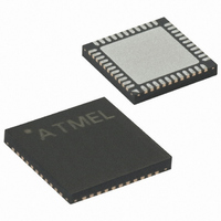
ATMEGA644V-10MU Atmel, ATMEGA644V-10MU Datasheet - Page 43

ATMEGA644V-10MU
Manufacturer Part Number
ATMEGA644V-10MU
Description
IC AVR MCU FLASH 64K 44-QFN
Manufacturer
Atmel
Series
AVR® ATmegar
Specifications of ATMEGA644V-10MU
Core Processor
AVR
Core Size
8-Bit
Speed
10MHz
Connectivity
I²C, SPI, UART/USART
Peripherals
Brown-out Detect/Reset, POR, PWM, WDT
Number Of I /o
32
Program Memory Size
64KB (32K x 16)
Program Memory Type
FLASH
Eeprom Size
2K x 8
Ram Size
4K x 8
Voltage - Supply (vcc/vdd)
1.8 V ~ 5.5 V
Data Converters
A/D 8x10b
Oscillator Type
Internal
Operating Temperature
-40°C ~ 85°C
Package / Case
44-VQFN Exposed Pad
Package
44QFN EP
Device Core
AVR
Family Name
ATmega
Maximum Speed
10 MHz
Operating Supply Voltage
2.5|3.3|5 V
Data Bus Width
8 Bit
Number Of Programmable I/os
32
Interface Type
JTAG/SPI/TWI/USART
On-chip Adc
8-chx10-bit
Number Of Timers
3
Processor Series
ATMEGA64x
Core
AVR8
Data Ram Size
4 KB
Maximum Clock Frequency
20 MHz
Maximum Operating Temperature
+ 85 C
Mounting Style
SMD/SMT
Minimum Operating Temperature
- 40 C
For Use With
ATSTK600-TQFP44 - STK600 SOCKET/ADAPTER 44-TQFPATSTK600 - DEV KIT FOR AVR/AVR32770-1007 - ISP 4PORT ATMEL AVR MCU SPI/JTAGATAVRISP2 - PROGRAMMER AVR IN SYSTEM
Lead Free Status / RoHS Status
Lead free / RoHS Compliant
Available stocks
Company
Part Number
Manufacturer
Quantity
Price
Part Number:
ATMEGA644V-10MU
Manufacturer:
ATMEL/爱特梅尔
Quantity:
20 000
- Current page: 43 of 376
- Download datasheet (8Mb)
8.10.7
8.11
8.11.1
2593N–AVR–07/10
Register Description
On-chip Debug System
SMCR – Sleep Mode Control Register
DIDR0). Refer to
Input Disable Register 0” on page 252
If the On-chip debug system is enabled by the OCDEN Fuse and the chip enters sleep mode,
the main clock source is enabled, and hence, always consumes power. In the deeper sleep
modes, this will contribute significantly to the total current consumption.
There are three alternative ways to disable the OCD system:
• Disable the OCDEN Fuse.
• Disable the JTAGEN Fuse.
• Write one to the JTD bit in MCUCR.
The Sleep Mode Control Register contains control bits for power management.
• Bits 3, 2, 1 – SM2:0: Sleep Mode Select Bits 2, 1, and 0
These bits select between the five available sleep modes as shown in
Table 8-2.
Note:
• Bit 0 – SE: Sleep Enable
The SE bit must be written to logic one to make the MCU enter the sleep mode when the SLEEP
instruction is executed. To avoid the MCU entering the sleep mode unless it is the programmer’s
purpose, it is recommended to write the Sleep Enable (SE) bit to one just before the execution of
the SLEEP instruction and to clear it immediately after waking up.
Bit
0x33 (0x53)
Read/Write
Initial Value
SM2
0
0
0
0
1
1
1
1
1. Standby modes are only recommended for use with external crystals or resonators.
Sleep Mode Select
7
–
R
0
”DIDR1 – Digital Input Disable Register 1” on page 232
SM1
0
0
1
1
0
0
1
1
6
–
R
0
R
5
–
0
SM0
0
1
0
1
0
1
0
1
for details.
R
4
–
0
Sleep Mode
Idle
ADC Noise Reduction
Power-down
Power-save
Reserved
Reserved
Standby
Extended Standby
SM2
R/W
3
0
(1)
SM1
R/W
2
0
(1)
SM0
R/W
Table
1
0
ATmega644
and
8-2.
”DIDR0 – Digital
R/W
SE
0
0
SMCR
43
Related parts for ATMEGA644V-10MU
Image
Part Number
Description
Manufacturer
Datasheet
Request
R

Part Number:
Description:
Manufacturer:
Atmel Corporation
Datasheet:

Part Number:
Description:
IC AVR MCU FLASH 64K 44-QFN
Manufacturer:
Atmel
Datasheet:

Part Number:
Description:
IC AVR MCU FLASH 64K 44TQFP
Manufacturer:
Atmel
Datasheet:

Part Number:
Description:
IC AVR MCU FLASH 64K 40DIP
Manufacturer:
Atmel
Datasheet:

Part Number:
Description:
MCU AVR 64K FLASH 20MHZ 44TQFP
Manufacturer:
Atmel
Datasheet:

Part Number:
Description:
MCU AVR 64K FLASH 20MHZ 44QFN
Manufacturer:
Atmel
Datasheet:

Part Number:
Description:
Atmega644 8-bit Avr Microcontroller With 64k Bytes In-system Programmable Flash
Manufacturer:
ATMEL Corporation
Datasheet:

Part Number:
Description:
Manufacturer:
Atmel Corporation
Datasheet:

Part Number:
Description:
Manufacturer:
ATMEL Corporation
Datasheet:

Part Number:
Description:
Manufacturer:
ATMEL Corporation
Datasheet:

Part Number:
Description:
IC AVR MCU 64K 16MHZ 5V 64TQFP
Manufacturer:
Atmel
Datasheet:

Part Number:
Description:
IC AVR MCU 64K 16MHZ 5V 64-QFN
Manufacturer:
Atmel
Datasheet:


