LPC3180FEL320,551 NXP Semiconductors, LPC3180FEL320,551 Datasheet - Page 21
LPC3180FEL320,551
Manufacturer Part Number
LPC3180FEL320,551
Description
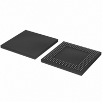
IC ARM9 MCU 208MHZ 320-LFBGA
Manufacturer
NXP Semiconductors
Series
LPC3000r
Specifications of LPC3180FEL320,551
Program Memory Type
ROMless
Package / Case
320-LFBGA
Core Processor
ARM9
Core Size
16/32-Bit
Speed
208MHz
Connectivity
EBI/EMI, I²C, MMC, SPI, UART/USART, USB OTG
Peripherals
DMA, PWM, WDT
Number Of I /o
55
Ram Size
64K x 8
Voltage - Supply (vcc/vdd)
1.1 V ~ 3.3 V
Data Converters
A/D 3x10b
Oscillator Type
External
Operating Temperature
-40°C ~ 85°C
Processor Series
LPC31
Core
ARM926EJ-S
Data Bus Width
16 bit, 32 bit
Data Ram Size
64 KB
Interface Type
I2C/SPI/UART/USB
Maximum Clock Frequency
208 MHz
Number Of Programmable I/os
55
Number Of Timers
2
Operating Supply Voltage
3 V
Maximum Operating Temperature
+ 85 C
Mounting Style
SMD/SMT
3rd Party Development Tools
MDK-ARM, RL-ARM, ULINK2, LPC3180-DEV-KIT
Development Tools By Supplier
OM10096
Minimum Operating Temperature
- 40 C
On-chip Adc
3-ch x 10-bit
Package
320LFBGA
Device Core
ARM926EJ-S
Family Name
LPC3100
Maximum Speed
208 MHz
Lead Free Status / RoHS Status
Lead free / RoHS Compliant
For Use With
622-1018 - EVAL KIT FOR LP3180568-4063 - KIT DEV LPC3180568-4062 - DEBUGGER J-LINK JTAG568-4061 - DEBUGGER U-LINK2 JTAG FOR NXP
Eeprom Size
-
Program Memory Size
-
Lead Free Status / Rohs Status
Lead free / RoHS Compliant
Other names
935281874551
LPC3180FEL320-S
LPC3180FEL320-S
LPC3180FEL320-S
LPC3180FEL320-S
Available stocks
Company
Part Number
Manufacturer
Quantity
Price
Company:

Part Number:
LPC3180FEL320,551
Manufacturer:
NXP Semiconductors
Quantity:
10 000


NXP Semiconductors
LPC3180_01_1
Preliminary data sheet
6.16.1 Features
6.17.1 Features
6.16 SD card controller
6.17 Keyboard scan
6.18 High-speed timer
The SD interface allows access to external SD memory cards. The SD card interface
conforms to the SD Memory Card Specification Version 1.01.
The keyboard scan function can automatically scan a keyboard of up to 64 keys in an
8 × 8 matrix. In operation, the keyboard scanner’s internal state machine will normally be
in an idle state, with all KEY_ROW[n] pins set high, waiting for a change in the column
inputs to indicate that one or more keys have been pressed.
When a keypress is detected, the matrix is scanned by setting one output pin high at a
time and reading the column inputs. After de-bouncing, the keypad state is stored and an
interrupt is generated. The keypad is then continuously scanned waiting for ‘extra key
pressed’ or ‘key released’. Any new keypad state is scanned and stored into the matrix
registers followed by a new interrupt request to the interrupt controller. It is possible to
detect and separate up to 64 multiple keys pressed.
The high-speed timer block is clocked by the main peripheral clock. The clock is first
divided down in a 16-bit programmable prescale counter which clocks a 32-bit
Timer/Counter.
•
•
•
•
•
•
•
•
•
•
•
•
•
•
•
DMA support for data transmit and receive.
1-bit to 16-bit word length.
Choice of LSB or MSB first data transmission.
64 × 16-bit input or output FIFO.
Bit rates up to 52 Mbit/s.
Busy input function.
DMA time out interrupt to allow detection of end of reception when using DMA.
Timed interrupt to facilitate emptying the FIFO at the end of a transmission.
SPI clock and data pins may be used as general purpose pins if the SPI is not used.
Conformance to the SD Memory Card Specification Version 1.01.
DMA is supported through the system DMA controller.
Provides all functions specific to the SD memory card. These include the clock
generation unit, power management control, command and data transfer.
Supports up to 64 keys in 8 × 8 matrix.
Programmable debounce period.
A key press can wake up the CPU from Stop mode.
Rev. 00.08 — 20 November 2008
16/32-bit ARM microcontroller with external memory interface
LPC3180/01
© NXP B.V. 2008. All rights reserved.
21 of 56
Related parts for LPC3180FEL320,551
Image
Part Number
Description
Manufacturer
Datasheet
Request
R

Part Number:
Description:
The LPC3180 is an ARM9-based microcontroller for embedded applications requiringhigh performance combined with low power dissipation
Manufacturer:
NXP Semiconductors
Datasheet:

Part Number:
Description:
MCU, MPU & DSP Development Tools LPC3180 Dev Kit
Manufacturer:
FDI

Part Number:
Description:
NXP Semiconductors designed the LPC2420/2460 microcontroller around a 16-bit/32-bitARM7TDMI-S CPU core with real-time debug interfaces that include both JTAG andembedded trace
Manufacturer:
NXP Semiconductors
Datasheet:

Part Number:
Description:
NXP Semiconductors designed the LPC2458 microcontroller around a 16-bit/32-bitARM7TDMI-S CPU core with real-time debug interfaces that include both JTAG andembedded trace
Manufacturer:
NXP Semiconductors
Datasheet:
Part Number:
Description:
NXP Semiconductors designed the LPC2468 microcontroller around a 16-bit/32-bitARM7TDMI-S CPU core with real-time debug interfaces that include both JTAG andembedded trace
Manufacturer:
NXP Semiconductors
Datasheet:
Part Number:
Description:
NXP Semiconductors designed the LPC2470 microcontroller, powered by theARM7TDMI-S core, to be a highly integrated microcontroller for a wide range ofapplications that require advanced communications and high quality graphic displays
Manufacturer:
NXP Semiconductors
Datasheet:
Part Number:
Description:
NXP Semiconductors designed the LPC2478 microcontroller, powered by theARM7TDMI-S core, to be a highly integrated microcontroller for a wide range ofapplications that require advanced communications and high quality graphic displays
Manufacturer:
NXP Semiconductors
Datasheet:
Part Number:
Description:
The Philips Semiconductors XA (eXtended Architecture) family of 16-bit single-chip microcontrollers is powerful enough to easily handle the requirements of high performance embedded applications, yet inexpensive enough to compete in the market for hi
Manufacturer:
NXP Semiconductors
Datasheet:
Part Number:
Description:
The XA-S3 device is a member of Philips Semiconductors? XA(eXtended Architecture) family of high performance 16-bitsingle-chip microcontrollers
Manufacturer:
NXP Semiconductors
Datasheet:

Part Number:
Description:
The NXP BlueStreak LH75401/LH75411 family consists of two low-cost 16/32-bit System-on-Chip (SoC) devices
Manufacturer:
NXP Semiconductors
Datasheet:
Part Number:
Description:
The NXP LPC3130/3131 combine an 180 MHz ARM926EJ-S CPU core, high-speed USB2
Manufacturer:
NXP Semiconductors
Datasheet:
Part Number:
Description:
The NXP LPC3141 combine a 270 MHz ARM926EJ-S CPU core, High-speed USB 2
Manufacturer:
NXP Semiconductors
Part Number:
Description:
The NXP LPC3143 combine a 270 MHz ARM926EJ-S CPU core, High-speed USB 2
Manufacturer:
NXP Semiconductors

Part Number:
Description:
The NXP LPC3152 combines an 180 MHz ARM926EJ-S CPU core, High-speed USB 2
Manufacturer:
NXP Semiconductors