P80C557E4EFB/01,55 NXP Semiconductors, P80C557E4EFB/01,55 Datasheet - Page 20
P80C557E4EFB/01,55
Manufacturer Part Number
P80C557E4EFB/01,55
Description
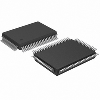
IC 80C51 MCU 1024 ROMLESS 80QFP
Manufacturer
NXP Semiconductors
Series
80Cr
Datasheet
1.P80C557E4EFB0155.pdf
(72 pages)
Specifications of P80C557E4EFB/01,55
Core Processor
8051
Core Size
8-Bit
Speed
16MHz
Connectivity
EBI/EMI, I²C, UART/USART
Peripherals
POR, PWM, WDT
Number Of I /o
40
Program Memory Type
ROMless
Ram Size
1K x 8
Voltage - Supply (vcc/vdd)
4.5 V ~ 5.5 V
Data Converters
A/D 8x10b
Oscillator Type
External
Operating Temperature
-40°C ~ 85°C
Package / Case
80-QFP
Processor Series
P80C5x
Core
80C51
Data Bus Width
8 bit
Data Ram Size
1 KB
Interface Type
I2C, UART
Maximum Clock Frequency
16 MHz
Number Of Programmable I/os
40
Number Of Timers
3
Maximum Operating Temperature
+ 85 C
Mounting Style
SMD/SMT
3rd Party Development Tools
PK51, CA51, A51, ULINK2
Minimum Operating Temperature
- 40 C
On-chip Adc
10 bit, 8 Channel
Lead Free Status / RoHS Status
Lead free / RoHS Compliant
Eeprom Size
-
Program Memory Size
-
Lead Free Status / Rohs Status
Details
Other names
935263156557
P80C557E4FB
P80C557E4FB
P80C557E4FB
P80C557E4FB
Available stocks
Company
Part Number
Manufacturer
Quantity
Price
Company:

Part Number:
P80C557E4EFB/01,55
Manufacturer:
IR
Quantity:
20
Company:
Part Number:
P80C557E4EFB/01,55
Manufacturer:
NXP Semiconductors
Quantity:
10 000


Philips Semiconductors
Digital Input Port Register P5
Port 5 Special Function Register P5 always represents the binary
value of the logic level at input pins P5.0/ADC0...P5.7/ADC7. P5 is
not affected by chip reset. P5 is a read only register. Its hardware
address is C7H. P5 is not bit addressable.
Reading Special Function Register P5 does not affect A/D
conversions. But it is recommended to use the digital input port
function of the hardware Port 5 only as an alternative to analog input
voltage conversions. Simultaneous mixed operation is discouraged
for the sake of A/D conversion result reliability and accuracy.
For further information on Port 5, refer to the “I/O facilities” section.
For further information on A/D Special Function Registers, refer to
the “Internal Data Memory” section.
Reset
After a RESET of the microcontroller the ADCON and ADPSS
register bits are initialized to zero. Registers ADRSLn and ADRSH
are not initialized by a RESET.
Idle and Power-down Mode
The A/D Converter is active only when the microcontroller is in
normal operating mode. If the Idle or Power-down Mode is activated,
then the ADC is switched off and put into a power saving idle state –
a conversion in progress is aborted, a previously set ADSST flag is
cleared and the internal clock is halted. The conversion result
registers are not affected.
The interrupt flag ADINT will not be set by activation of Idle or
Power-down Mode. A previously set flag ADINT will not be cleared
by the hardware. (Note: ADINT cannot be cleared by hardware at
all, except for a RESET – it must be cleared by the user software.)
After a wakeup from Idle or Power-down Mode a set flag ADINT
indicates that at least one autoscan loop was finished completely
before the microcontroller was put into the respective power
reduction mode and it indicates that the stored result data may be
fetched now – if desired.
For further information on Idle and Power-down Mode, refer to the
“Power reduction modes” section.
Timing
A programmable prescaler is controlled by the bits ADPR1 and
ADPR0 in register ADCON to adapt the conversion time for different
microcontroller clock frequencies.
Table 11 shows conversion times (tconv) for one A/D conversion at
some convenient system clock frequencies (fclk) and ADC prescaler
divisors (m), which are user selectable by the bits ADCON.7/ADPR1
and ADCON.6/ADPR0.
1999 Mar 02
Single-chip 8-bit microcontroller
P5 (C7H)
P5.7
7
P5.6
6
Figure 18. Digital input port register P5.
P5.5
5
20
P5.4
4
P83C557E4/P80C557E4/P89C557E4
Conversion time tconv = (6 m + 1) machine cycles
For conversion times outside the limits for tconv the specified ADC
characteristics are not guaranteed; (prohibited conversion times are
put in brackets):
Table 11. Conversion time configuration
A conversion time tconv consists of one sample time period (which
equals two bit conversion times), 10 bit conversion time periods and
one machine cycle to store the result.
After result storage an extra initializing time period follows to select
the next analog input channel (according to the contents of SFR
ADPSS), before the input signal is sampled.
Thus the time period between two adjacent conversions within an
autoscan loop is larger than the pure time tconv. This autoscan cycle
time is ( 7 m ) machine cycles.
At the start of an autoscan conversion the time between writing to
SFR ADCON and the first analog input signal sampling depends on
the current prescaler value (m) and the relative time offset between
this write operation and the internal (divided) ADC clock. This gives
a variation range for the A/D conversion start time of ( m / 2 )
machine cycles.
m
2
4
6
8
P5.3
examples (tconv/ s)
3
6 MHz
[74]
[98]
26
50
P5.2
2
8 MHz
[55.5]
[73.5]
19.5
37.5
f
CLK
P5.1
1
12 MHz
[13]
25
37
49
Product specification
P5.0
0
16 MHz
[9.75]
18.75
27.75
36.75
Related parts for P80C557E4EFB/01,55
Image
Part Number
Description
Manufacturer
Datasheet
Request
R

Part Number:
Description:
NXP Semiconductors designed the LPC2420/2460 microcontroller around a 16-bit/32-bitARM7TDMI-S CPU core with real-time debug interfaces that include both JTAG andembedded trace
Manufacturer:
NXP Semiconductors
Datasheet:

Part Number:
Description:
NXP Semiconductors designed the LPC2458 microcontroller around a 16-bit/32-bitARM7TDMI-S CPU core with real-time debug interfaces that include both JTAG andembedded trace
Manufacturer:
NXP Semiconductors
Datasheet:
Part Number:
Description:
NXP Semiconductors designed the LPC2468 microcontroller around a 16-bit/32-bitARM7TDMI-S CPU core with real-time debug interfaces that include both JTAG andembedded trace
Manufacturer:
NXP Semiconductors
Datasheet:
Part Number:
Description:
NXP Semiconductors designed the LPC2470 microcontroller, powered by theARM7TDMI-S core, to be a highly integrated microcontroller for a wide range ofapplications that require advanced communications and high quality graphic displays
Manufacturer:
NXP Semiconductors
Datasheet:
Part Number:
Description:
NXP Semiconductors designed the LPC2478 microcontroller, powered by theARM7TDMI-S core, to be a highly integrated microcontroller for a wide range ofapplications that require advanced communications and high quality graphic displays
Manufacturer:
NXP Semiconductors
Datasheet:
Part Number:
Description:
The Philips Semiconductors XA (eXtended Architecture) family of 16-bit single-chip microcontrollers is powerful enough to easily handle the requirements of high performance embedded applications, yet inexpensive enough to compete in the market for hi
Manufacturer:
NXP Semiconductors
Datasheet:
Part Number:
Description:
The XA-S3 device is a member of Philips Semiconductors? XA(eXtended Architecture) family of high performance 16-bitsingle-chip microcontrollers
Manufacturer:
NXP Semiconductors
Datasheet:

Part Number:
Description:
The NXP BlueStreak LH75401/LH75411 family consists of two low-cost 16/32-bit System-on-Chip (SoC) devices
Manufacturer:
NXP Semiconductors
Datasheet:
Part Number:
Description:
The NXP LPC3130/3131 combine an 180 MHz ARM926EJ-S CPU core, high-speed USB2
Manufacturer:
NXP Semiconductors
Datasheet:
Part Number:
Description:
The NXP LPC3141 combine a 270 MHz ARM926EJ-S CPU core, High-speed USB 2
Manufacturer:
NXP Semiconductors
Part Number:
Description:
The NXP LPC3143 combine a 270 MHz ARM926EJ-S CPU core, High-speed USB 2
Manufacturer:
NXP Semiconductors

Part Number:
Description:
The NXP LPC3152 combines an 180 MHz ARM926EJ-S CPU core, High-speed USB 2
Manufacturer:
NXP Semiconductors
Part Number:
Description:
The NXP LPC3154 combines an 180 MHz ARM926EJ-S CPU core, High-speed USB 2
Manufacturer:
NXP Semiconductors

Part Number:
Description:
Standard level N-channel enhancement mode Field-Effect Transistor (FET) in a plastic package using NXP High-Performance Automotive (HPA) TrenchMOS technology
Manufacturer:
NXP Semiconductors
Datasheet: