ST7FOXK1T6TR STMicroelectronics, ST7FOXK1T6TR Datasheet - Page 161
ST7FOXK1T6TR
Manufacturer Part Number
ST7FOXK1T6TR
Description
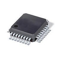
IC MCU 8BIT 4K FLASH 20LQFP
Manufacturer
STMicroelectronics
Series
ST7r
Datasheet
1.ST7FOXF1M6.pdf
(226 pages)
Specifications of ST7FOXK1T6TR
Core Processor
ST7
Core Size
8-Bit
Speed
8MHz
Connectivity
I²C
Peripherals
LVD, POR, PWM, WDT
Number Of I /o
24
Program Memory Size
4KB (4K x 8)
Program Memory Type
FLASH
Ram Size
384 x 8
Voltage - Supply (vcc/vdd)
4.5 V ~ 5.5 V
Data Converters
A/D 10x10b
Oscillator Type
Internal
Operating Temperature
-40°C ~ 85°C
Package / Case
32-LQFP
Processor Series
ST7FOXx
Core
ST7
Data Bus Width
8 bit
Data Ram Size
384 B
Interface Type
I2C
Maximum Clock Frequency
8 MHz
Number Of Programmable I/os
24
Number Of Timers
4
Maximum Operating Temperature
+ 85 C
Mounting Style
SMD/SMT
Development Tools By Supplier
ST7FLITE-SK/RAIS, STX-RLINK
Minimum Operating Temperature
- 40 C
On-chip Adc
10 bit, 1 Channel
For Use With
497-5049 - KIT STARTER RAISONANCE ST7FLITE
Lead Free Status / RoHS Status
Lead free / RoHS Compliant
Eeprom Size
-
Lead Free Status / Rohs Status
Details
Available stocks
Company
Part Number
Manufacturer
Quantity
Price
Company:

Part Number:
ST7FOXK1T6TR
Manufacturer:
STMicroelectronics
Quantity:
10 000


ST7FOXF1, ST7FOXK1, ST7FOXK2
Note:
Note:
Note:
Caution:
Figure 75. Generic SS timing diagram
Figure 76. Hardware/software slave select management
Master mode operation
In master mode, the serial clock is output on the SCK pin. The clock frequency, polarity and
phase are configured by software (refer to the description of the SPICSR register).
The idle state of SCK must correspond to the polarity selected in the SPICSR register (by
pulling up SCK if CPOL = 1 or pulling down SCK if CPOL = 0).
How to operate the SPI in master mode
To operate the SPI in master mode, perform the following steps in order:
1.
The slave must have the same CPOL and CPHA settings as the master.
2.
3.
MSTR and SPE bits remain set only if SS is high).
if the SPICSR register is not written first, the SPICR register setting (MSTR bit) may be not
taken into account.
The transmit sequence begins when software writes a byte in the SPIDR register.
Write to the SPICR register:
–
–
Write to the SPICSR register:
–
Write to the SPICR register:
–
MOSI/MISO
Master SS
Slave SS
(if CPHA = 0)
Slave SS
(if CPHA = 1)
Select the clock frequency by configuring the SPR[2:0] bits.
Select the clock polarity and clock phase by configuring the CPOL and CPHA bits.
Figure 77
Either set the SSM bit and set the SSI bit or clear the SSM bit and tie the SS pin
high for the complete byte transmit sequence.
Set the MSTR and SPE bits
shows the four possible configurations.
SS
external pin
SSI bit
Byte 1
SSM bit
1
0
Byte 2
SS
internal
Byte 3
On-chip peripherals
161/226
Related parts for ST7FOXK1T6TR
Image
Part Number
Description
Manufacturer
Datasheet
Request
R

Part Number:
Description:
Low cost flash 8bit micro
Manufacturer:
STMicroelectronics
Datasheet:
Part Number:
Description:
STMicroelectronics [RIPPLE-CARRY BINARY COUNTER/DIVIDERS]
Manufacturer:
STMicroelectronics
Datasheet:
Part Number:
Description:
STMicroelectronics [LIQUID-CRYSTAL DISPLAY DRIVERS]
Manufacturer:
STMicroelectronics
Datasheet:

Part Number:
Description:
BOARD EVAL FOR MEMS SENSORS
Manufacturer:
STMicroelectronics
Datasheet:
Part Number:
Description:
NPN TRANSISTOR POWER MODULE
Manufacturer:
STMicroelectronics
Datasheet:
Part Number:
Description:
TURBOSWITCH ULTRA-FAST HIGH VOLTAGE DIODE
Manufacturer:
STMicroelectronics
Datasheet:
Part Number:
Description:
Manufacturer:
STMicroelectronics
Datasheet:
Part Number:
Description:
DIODE / SCR MODULE
Manufacturer:
STMicroelectronics
Datasheet:
Part Number:
Description:
DIODE / SCR MODULE
Manufacturer:
STMicroelectronics
Datasheet:
Part Number:
Description:
Search -----> STE16N100
Manufacturer:
STMicroelectronics
Datasheet:
Part Number:
Description:
Search ---> STE53NA50
Manufacturer:
STMicroelectronics
Datasheet:
Part Number:
Description:
NPN Transistor Power Module
Manufacturer:
STMicroelectronics
Datasheet: