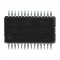
Z8F0813HJ005EG Zilog, Z8F0813HJ005EG Datasheet - Page 162

Z8F0813HJ005EG
Manufacturer Part Number
Z8F0813HJ005EG
Description
IC Z8 ENCORE MCU FLASH 8K 28SSOP
Manufacturer
Zilog
Series
Encore!® XP®r
Datasheet
1.Z8F0813PH005SC.pdf
(227 pages)
Specifications of Z8F0813HJ005EG
Core Processor
Z8
Core Size
8-Bit
Speed
5MHz
Connectivity
IrDA, UART/USART
Peripherals
Brown-out Detect/Reset, LED, POR, PWM, WDT
Number Of I /o
24
Program Memory Size
8KB (8K x 8)
Program Memory Type
FLASH
Ram Size
1K x 8
Voltage - Supply (vcc/vdd)
2.7 V ~ 3.6 V
Oscillator Type
Internal
Operating Temperature
-40°C ~ 105°C
Package / Case
28-SSOP
Lead Free Status / RoHS Status
Lead free / RoHS Compliant
Eeprom Size
-
Data Converters
-
Other names
269-4182
Z8F0813HJ005EG
Z8F0813HJ005EG
- Current page: 162 of 227
- Download datasheet (3Mb)
PS025203-0405
•
•
•
•
•
Write Program Counter (06H)—The Write Program Counter command writes the data
that follows to the eZ8 CPU’s Program Counter (PC). If the device is not in DEBUG mode
or if the Flash Read Protect Option bit is enabled, the Program Counter (PC) values are
discarded.
DBG
DBG
DBG
Read Program Counter (07H)—The Read Program Counter command reads the value
in the eZ8 CPU’s Program Counter (PC). If the device is not in DEBUG mode or if the
Flash Read Protect Option bit is enabled, this command returns
DBG
DBG
DBG
Write Register (08H)—The Write Register command writes data to the Register File.
Data can be written 1–256 bytes at a time (256 bytes can be written by setting size to 0). If
the device is not in DEBUG mode, the address and data values are discarded. If the Flash
Read Protect Option bit is enabled, only writes to the Flash Control Registers are allowed
and all other register write data values are discarded.
DBG
DBG
DBG
DBG
DBG
Read Register (09H)—The Read Register command reads data from the Register File.
Data can be read 1–256 bytes at a time (256 bytes can be read by setting size to 0). If the
device is not in DEBUG mode or if the Flash Read Protect Option bit is enabled, this com-
mand returns
DBG
DBG
DBG
DBG
DBG
Write Program Memory (0AH)—The Write Program Memory command writes data
to Program Memory. This command is equivalent to the LDC and LDCI instructions. Data
can be written 1–65536 bytes at a time (65536 bytes can be written by setting size to 0).
The on-chip Flash Controller must be written to and unlocked for the programming oper-
ation to occur. If the Flash Controller is not unlocked, the data is discarded. If the device
is not in DEBUG mode or if the Flash Read Protect Option bit is enabled, the data is dis-
carded.
←
←
←
←
→
→
←
←
←
←
←
←
←
←
←
→
06H
ProgramCounter[15:8]
ProgramCounter[7:0]
07H
ProgramCounter[15:8]
ProgramCounter[7:0]
08H
{4’h0,Register Address[11:8]}
Register Address[7:0]
Size[7:0]
1-256 data bytes
09H
{4’h0,Register Address[11:8]
Register Address[7:0]
Size[7:0]
1-256 data bytes
FFH
for all the data values.
P R E L I M I N A R Y
Z8 Encore!
Product Specification
FFFFH
®
Z8F0823 Series
.
On-Chip Debugger
145
Related parts for Z8F0813HJ005EG
Image
Part Number
Description
Manufacturer
Datasheet
Request
R

Part Number:
Description:
Communication Controllers, ZILOG INTELLIGENT PERIPHERAL CONTROLLER (ZIP)
Manufacturer:
Zilog, Inc.
Datasheet:

Part Number:
Description:
KIT DEV FOR Z8 ENCORE 16K TO 64K
Manufacturer:
Zilog
Datasheet:

Part Number:
Description:
KIT DEV Z8 ENCORE XP 28-PIN
Manufacturer:
Zilog
Datasheet:

Part Number:
Description:
DEV KIT FOR Z8 ENCORE 8K/4K
Manufacturer:
Zilog
Datasheet:

Part Number:
Description:
KIT DEV Z8 ENCORE XP 28-PIN
Manufacturer:
Zilog
Datasheet:

Part Number:
Description:
DEV KIT FOR Z8 ENCORE 4K TO 8K
Manufacturer:
Zilog
Datasheet:

Part Number:
Description:
CMOS Z8 microcontroller. ROM 16 Kbytes, RAM 256 bytes, speed 16 MHz, 32 lines I/O, 3.0V to 5.5V
Manufacturer:
Zilog, Inc.
Datasheet:

Part Number:
Description:
Low-cost microcontroller. 512 bytes ROM, 61 bytes RAM, 8 MHz
Manufacturer:
Zilog, Inc.
Datasheet:

Part Number:
Description:
Z8 4K OTP Microcontroller
Manufacturer:
Zilog, Inc.
Datasheet:

Part Number:
Description:
CMOS SUPER8 ROMLESS MCU
Manufacturer:
Zilog, Inc.
Datasheet:

Part Number:
Description:
SL1866 CMOSZ8 OTP Microcontroller
Manufacturer:
Zilog, Inc.
Datasheet:

Part Number:
Description:
SL1866 CMOSZ8 OTP Microcontroller
Manufacturer:
Zilog, Inc.
Datasheet:

Part Number:
Description:
OTP (KB) = 1, RAM = 125, Speed = 12, I/O = 14, 8-bit Timers = 2, Comm Interfaces Other Features = Por, LV Protect, Voltage = 4.5-5.5V
Manufacturer:
Zilog, Inc.
Datasheet:

Part Number:
Description:
Manufacturer:
Zilog, Inc.
Datasheet:


