R5F21292SNSP#U0 Renesas Electronics America, R5F21292SNSP#U0 Datasheet - Page 202
R5F21292SNSP#U0
Manufacturer Part Number
R5F21292SNSP#U0
Description
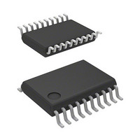
MCU 3/5V 16K+2K 20PIN-SSOP
Manufacturer
Renesas Electronics America
Series
M16C™ M16C/R8C/Tiny/29r
Datasheet
1.R5F21282SNSPU0.pdf
(473 pages)
Specifications of R5F21292SNSP#U0
Core Processor
R8C
Core Size
16-Bit
Speed
20MHz
Connectivity
I²C, LIN, SIO, SSU, UART/USART
Peripherals
LED, POR, Voltage Detect, WDT
Number Of I /o
13
Program Memory Size
8KB (8K x 8)
Program Memory Type
FLASH
Ram Size
512 x 8
Voltage - Supply (vcc/vdd)
2.2 V ~ 5.5 V
Data Converters
A/D 4x10b
Oscillator Type
Internal
Operating Temperature
-20°C ~ 85°C
Package / Case
20-SSOP
For Use With
R0K521276S000BE - KIT DEV RSK-R8C/26-29
Lead Free Status / RoHS Status
Lead free / RoHS Compliant
Eeprom Size
-
Available stocks
Company
Part Number
Manufacturer
Quantity
Price


R8C/28 Group, R8C/29 Group
Rev.2.10
REJ09B0279-0210
Figure 14.35
Timer RC Output Master Enable Register
b7 b6 b5 b4
NOTE:
1.
These bits are disabled for input pins set to the input capture function.
Sep 26, 2008
b3 b2
TRCOER Register
b1 b0
Bit Symbol
TRCOER
(b6-b4)
Symbol
PTO
Page 183 of 441
EA
EB
EC
ED
—
TRCIOA output disable bit
TRCIOB output disable bit
TRCIOC output disable bit
TRCIOD output disable bit
Nothing is assigned. If necessary, set to 0.
When read, the content is 1.
_____
INT0
cutoff signal input enabled
bit
of pulse output forced
Address
Bit Name
0132h
(1)
(1)
(1)
(1)
0 : Enable output
1 : Disable output (The TRCIOA pin is
0 : Enable output
1 : Disable output (The TRCIOB pin is
0 : Enable output
1 : Disable output (The TRCIOC pin is
0 : Enable output
1 : Disable output (The TRCIOD pin is
0 : Pulse output forced cutoff input disabled
1 : Pulse output forced cutoff input enabled
used as a programmable I/O port.)
used as a programmable I/O port.)
used as a programmable I/O port.)
used as a programmable I/O port.)
(Bits EA, EB, EC, and ED are set to 1
(disable output) w hen “L” is applied to the
_____
INT0
pin)
After Reset
01111111b
Function
14. Timers
RW
RW
RW
RW
RW
RW
—
Related parts for R5F21292SNSP#U0
Image
Part Number
Description
Manufacturer
Datasheet
Request
R

Part Number:
Description:
KIT STARTER FOR M16C/29
Manufacturer:
Renesas Electronics America
Datasheet:

Part Number:
Description:
KIT STARTER FOR R8C/2D
Manufacturer:
Renesas Electronics America
Datasheet:

Part Number:
Description:
R0K33062P STARTER KIT
Manufacturer:
Renesas Electronics America
Datasheet:

Part Number:
Description:
KIT STARTER FOR R8C/23 E8A
Manufacturer:
Renesas Electronics America
Datasheet:

Part Number:
Description:
KIT STARTER FOR R8C/25
Manufacturer:
Renesas Electronics America
Datasheet:

Part Number:
Description:
KIT STARTER H8S2456 SHARPE DSPLY
Manufacturer:
Renesas Electronics America
Datasheet:

Part Number:
Description:
KIT STARTER FOR R8C38C
Manufacturer:
Renesas Electronics America
Datasheet:

Part Number:
Description:
KIT STARTER FOR R8C35C
Manufacturer:
Renesas Electronics America
Datasheet:

Part Number:
Description:
KIT STARTER FOR R8CL3AC+LCD APPS
Manufacturer:
Renesas Electronics America
Datasheet:
Part Number:
Description:
KIT STARTER FOR RX610
Manufacturer:
Renesas Electronics America
Datasheet:

Part Number:
Description:
KIT STARTER FOR R32C/118
Manufacturer:
Renesas Electronics America
Datasheet:

Part Number:
Description:
KIT DEV RSK-R8C/26-29
Manufacturer:
Renesas Electronics America
Datasheet:

Part Number:
Description:
KIT STARTER FOR SH7124
Manufacturer:
Renesas Electronics America
Datasheet:

Part Number:
Description:
KIT STARTER FOR H8SX/1622
Manufacturer:
Renesas Electronics America
Datasheet:

Part Number:
Description:
KIT DEV FOR SH7203
Manufacturer:
Renesas Electronics America
Datasheet: