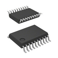
R5F21292SNSP#U0 Renesas Electronics America, R5F21292SNSP#U0 Datasheet - Page 22

R5F21292SNSP#U0
Manufacturer Part Number
R5F21292SNSP#U0
Description
MCU 3/5V 16K+2K 20PIN-SSOP
Manufacturer
Renesas Electronics America
Series
M16C™ M16C/R8C/Tiny/29r
Datasheet
1.R5F21282SNSPU0.pdf
(473 pages)
Specifications of R5F21292SNSP#U0
Core Processor
R8C
Core Size
16-Bit
Speed
20MHz
Connectivity
I²C, LIN, SIO, SSU, UART/USART
Peripherals
LED, POR, Voltage Detect, WDT
Number Of I /o
13
Program Memory Size
8KB (8K x 8)
Program Memory Type
FLASH
Ram Size
512 x 8
Voltage - Supply (vcc/vdd)
2.2 V ~ 5.5 V
Data Converters
A/D 4x10b
Oscillator Type
Internal
Operating Temperature
-20°C ~ 85°C
Package / Case
20-SSOP
For Use With
R0K521276S000BE - KIT DEV RSK-R8C/26-29
Lead Free Status / RoHS Status
Lead free / RoHS Compliant
Eeprom Size
-
Available stocks
Company
Part Number
Manufacturer
Quantity
Price
- Current page: 22 of 473
- Download datasheet (5Mb)
R8C/28 Group, R8C/29 Group
Rev.2.10
REJ09B0279-0210
Table 1.2
NOTES:
CPU
Peripheral
Functions
Electrical
Characteristics
Flash Memory
Operating Ambient Temperature
Package
1. I
2. Specify the D, K version if D, K version functions are to be used.
2
C bus is a trademark of Koninklijke Philips Electronics N. V.
Sep 26, 2008
Functions and Specifications for R8C/29 Group
Number of fundamental
instructions
Minimum instruction
execution time
Operating mode
Address space
Memory capacity
Ports
LED drive ports
Timers
Serial interfaces
Clock synchronous serial
interface
LIN module
A/D converter
Watchdog timer
Interrupts
Clock generation circuits
Oscillation stop detection
function
Voltage detection circuit
Power-on reset circuit
Supply voltage
Current consumption
(N, D version)
voltage
Programming and erasure
endurance
Programming and erasure
Item
Page 3 of 441
89 instructions
50 ns (f(XIN) = 20 MHz, VCC = 3.0 to 5.5 V) (other than K version)
62.5 ns (f(XIN) = 16 MHz, VCC = 3.0 to 5.5 V) (K version)
100 ns (f(XIN) = 10 MHz, VCC = 2.7 to 5.5 V)
200 ns (f(XIN) = 5 MHz, VCC = 2.2 to 5.5 V) (N, D version)
Single-chip
1 Mbyte
Refer to Table 1.4 Product Information for R8C/29 Group
I/O ports: 13 pins, Input port: 3 pins
I/O ports: 8 pins (N, D version)
Timer RA: 8 bits × 1 channel
Timer RB: 8 bits × 1 channel
Timer RC: 16 bits × 1 channel
Timer RE: With real-time clock and compare match function
1 channel (UART0): Clock synchronous serial I/O, UART
1 channel (UART1): UART
1 channel
Hardware LIN: 1 channel (timer RA, UART0)
10-bit A/D converter: 1 circuit, 4 channels
15 bits × 1 channel (with prescaler)
Internal: 15 sources (N, D version), Internal: 14 sources (J, K version)
External: 4 sources, Software: 4 sources, Priority levels: 7 levels
3 circuits
• XIN clock generation circuit (with on-chip feedback resistor)
• On-chip oscillator (high speed, low speed)
• XCIN clock generation circuit (32 kHz) (N, D version)
• Real-time clock (timer RE) (N, D version)
XIN clock oscillation stop detection function
On-chip
On-chip
VCC = 3.0 to 5.5 V (f(XIN) = 20 MHz) (other than K version)
VCC = 3.0 to 5.5 V (f(XIN) = 16 MHz) (K version)
VCC = 2.7 to 5.5 V (f(XIN) = 10 MHz)
VCC = 2.2 to 5.5 V (f(XIN) = 5 MHz) (N, D version)
Typ. 10 mA (VCC = 5.0 V, f(XIN) = 20 MHz)
Typ. 6 mA (VCC = 3.0 V, f(XIN) = 10 MHz)
Typ. 2.0 µA (VCC = 3.0 V, wait mode (f(XCIN) = 32 kHz)
Typ. 0.7 µA (VCC = 3.0 V, stop mode)
VCC = 2.7 to 5.5 V
10,000 times (data flash)
1,000 times (program ROM)
-20 to 85°C (N version)
-40 to 85°C (D, J version)
20-pin molded-plastic LSSOP
High-speed on-chip oscillator has a frequency adjustment function
I
Clock synchronous serial I/O with chip select
Reset start selectable
2
C bus Interface
(Each timer equipped with 8-bit prescaler)
(Input capture and output compare circuits)
(For J, K version, compare match function only.)
(1)
(2)
, -40 to 125°C (K version)
Specification
(2)
1. Overview
Related parts for R5F21292SNSP#U0
Image
Part Number
Description
Manufacturer
Datasheet
Request
R

Part Number:
Description:
KIT STARTER FOR M16C/29
Manufacturer:
Renesas Electronics America
Datasheet:

Part Number:
Description:
KIT STARTER FOR R8C/2D
Manufacturer:
Renesas Electronics America
Datasheet:

Part Number:
Description:
R0K33062P STARTER KIT
Manufacturer:
Renesas Electronics America
Datasheet:

Part Number:
Description:
KIT STARTER FOR R8C/23 E8A
Manufacturer:
Renesas Electronics America
Datasheet:

Part Number:
Description:
KIT STARTER FOR R8C/25
Manufacturer:
Renesas Electronics America
Datasheet:

Part Number:
Description:
KIT STARTER H8S2456 SHARPE DSPLY
Manufacturer:
Renesas Electronics America
Datasheet:

Part Number:
Description:
KIT STARTER FOR R8C38C
Manufacturer:
Renesas Electronics America
Datasheet:

Part Number:
Description:
KIT STARTER FOR R8C35C
Manufacturer:
Renesas Electronics America
Datasheet:

Part Number:
Description:
KIT STARTER FOR R8CL3AC+LCD APPS
Manufacturer:
Renesas Electronics America
Datasheet:

Part Number:
Description:
KIT STARTER FOR RX610
Manufacturer:
Renesas Electronics America
Datasheet:

Part Number:
Description:
KIT STARTER FOR R32C/118
Manufacturer:
Renesas Electronics America
Datasheet:

Part Number:
Description:
KIT DEV RSK-R8C/26-29
Manufacturer:
Renesas Electronics America
Datasheet:

Part Number:
Description:
KIT STARTER FOR SH7124
Manufacturer:
Renesas Electronics America
Datasheet:

Part Number:
Description:
KIT STARTER FOR H8SX/1622
Manufacturer:
Renesas Electronics America
Datasheet:

Part Number:
Description:
KIT DEV FOR SH7203
Manufacturer:
Renesas Electronics America
Datasheet:


