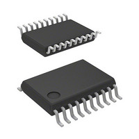
R5F21292SNSP#U0 Renesas Electronics America, R5F21292SNSP#U0 Datasheet - Page 325

R5F21292SNSP#U0
Manufacturer Part Number
R5F21292SNSP#U0
Description
MCU 3/5V 16K+2K 20PIN-SSOP
Manufacturer
Renesas Electronics America
Series
M16C™ M16C/R8C/Tiny/29r
Datasheet
1.R5F21282SNSPU0.pdf
(473 pages)
Specifications of R5F21292SNSP#U0
Core Processor
R8C
Core Size
16-Bit
Speed
20MHz
Connectivity
I²C, LIN, SIO, SSU, UART/USART
Peripherals
LED, POR, Voltage Detect, WDT
Number Of I /o
13
Program Memory Size
8KB (8K x 8)
Program Memory Type
FLASH
Ram Size
512 x 8
Voltage - Supply (vcc/vdd)
2.2 V ~ 5.5 V
Data Converters
A/D 4x10b
Oscillator Type
Internal
Operating Temperature
-20°C ~ 85°C
Package / Case
20-SSOP
For Use With
R0K521276S000BE - KIT DEV RSK-R8C/26-29
Lead Free Status / RoHS Status
Lead free / RoHS Compliant
Eeprom Size
-
Available stocks
Company
Part Number
Manufacturer
Quantity
Price
- Current page: 325 of 473
- Download datasheet (5Mb)
R8C/28 Group, R8C/29 Group
Rev.2.10
REJ09B0279-0210
Figure 16.43
16.3.5
The states of pins SCL and SDA are routed through the noise canceller before being latched internally.
Figure 16.43 shows a Block Diagram of Noise Canceller.
The noise canceller consists of two cascaded latch and match detector circuits. When the SCL pin input signal
(or SDA pin input signal) is sampled on f1 and two latch outputs match, the level is passed forward to the next
circuit. When they do not match, the former value is retained.
f1 (sampling clock)
Sep 26, 2008
Noise Canceller
SCL or SDA
input signal
Block Diagram of Noise Canceller
Page 306 of 441
f1 (sampling clock)
Period of f1
D
Latch
C
Q
D
Latch
C
Q
16. Clock Synchronous Serial Interface
detection
Match
circuit
Internal SCL
or SDA signal
Related parts for R5F21292SNSP#U0
Image
Part Number
Description
Manufacturer
Datasheet
Request
R

Part Number:
Description:
KIT STARTER FOR M16C/29
Manufacturer:
Renesas Electronics America
Datasheet:

Part Number:
Description:
KIT STARTER FOR R8C/2D
Manufacturer:
Renesas Electronics America
Datasheet:

Part Number:
Description:
R0K33062P STARTER KIT
Manufacturer:
Renesas Electronics America
Datasheet:

Part Number:
Description:
KIT STARTER FOR R8C/23 E8A
Manufacturer:
Renesas Electronics America
Datasheet:

Part Number:
Description:
KIT STARTER FOR R8C/25
Manufacturer:
Renesas Electronics America
Datasheet:

Part Number:
Description:
KIT STARTER H8S2456 SHARPE DSPLY
Manufacturer:
Renesas Electronics America
Datasheet:

Part Number:
Description:
KIT STARTER FOR R8C38C
Manufacturer:
Renesas Electronics America
Datasheet:

Part Number:
Description:
KIT STARTER FOR R8C35C
Manufacturer:
Renesas Electronics America
Datasheet:

Part Number:
Description:
KIT STARTER FOR R8CL3AC+LCD APPS
Manufacturer:
Renesas Electronics America
Datasheet:

Part Number:
Description:
KIT STARTER FOR RX610
Manufacturer:
Renesas Electronics America
Datasheet:

Part Number:
Description:
KIT STARTER FOR R32C/118
Manufacturer:
Renesas Electronics America
Datasheet:

Part Number:
Description:
KIT DEV RSK-R8C/26-29
Manufacturer:
Renesas Electronics America
Datasheet:

Part Number:
Description:
KIT STARTER FOR SH7124
Manufacturer:
Renesas Electronics America
Datasheet:

Part Number:
Description:
KIT STARTER FOR H8SX/1622
Manufacturer:
Renesas Electronics America
Datasheet:

Part Number:
Description:
KIT DEV FOR SH7203
Manufacturer:
Renesas Electronics America
Datasheet:


