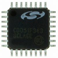
C8051F343-GQ Silicon Laboratories Inc, C8051F343-GQ Datasheet - Page 271

C8051F343-GQ
Manufacturer Part Number
C8051F343-GQ
Description
IC 8051 MCU FLASH 32K 32LQFP
Manufacturer
Silicon Laboratories Inc
Series
C8051F34xr
Specifications of C8051F343-GQ
Program Memory Type
FLASH
Program Memory Size
32KB (32K x 8)
Package / Case
32-LQFP
Core Processor
8051
Core Size
8-Bit
Speed
48MHz
Connectivity
SMBus (2-Wire/I²C), SPI, UART/USART, USB
Peripherals
Brown-out Detect/Reset, POR, PWM, Temp Sensor, WDT
Number Of I /o
25
Ram Size
2.25K x 8
Voltage - Supply (vcc/vdd)
2.7 V ~ 3.6 V
Data Converters
A/D 21x10b
Oscillator Type
Internal
Operating Temperature
-40°C ~ 85°C
Processor Series
C8051F3x
Core
8051
Data Bus Width
8 bit
Data Ram Size
2304 B
Interface Type
I2C, SMBus, SPI, UART, USB
Maximum Clock Frequency
48 MHz
Number Of Programmable I/os
25
Number Of Timers
4
Operating Supply Voltage
2.7 V to 5.25 V
Maximum Operating Temperature
+ 85 C
Mounting Style
SMD/SMT
3rd Party Development Tools
KSK-SL-F34X, KSK-SL-TOOLSTICK, PK51, CA51, A51, ULINK2
Development Tools By Supplier
C8051F340DK
Minimum Operating Temperature
- 40 C
On-chip Adc
10 bit, 17 Channel
Package
32LQFP
Device Core
8051
Family Name
C8051F34x
Maximum Speed
48 MHz
Data Rom Size
128 B
A/d Bit Size
10 bit
A/d Channels Available
17
Height
1.4 mm
Length
7 mm
Supply Voltage (max)
3.6 V
Supply Voltage (min)
2.7 V
Width
7 mm
Lead Free Status / RoHS Status
Lead free / RoHS Compliant
For Use With
336-1748 - ADAPTER TOOLSTICK FOR C8051F34X770-1006 - ISP 4PORT FOR SILABS C8051F MCU
Eeprom Size
-
Lead Free Status / Rohs Status
Lead free / RoHS Compliant
Other names
336-1301
Available stocks
Company
Part Number
Manufacturer
Quantity
Price
Company:
Part Number:
C8051F343-GQ
Manufacturer:
Silicon Laboratories Inc
Quantity:
10 000
Company:
Part Number:
C8051F343-GQR
Manufacturer:
Silicon Laboratories Inc
Quantity:
10 000
- Current page: 271 of 276
- Download datasheet (2Mb)
23. C2 Interface
C8051F34x devices include an on-chip Silicon Labs 2-Wire (C2) debug interface to allow Flash program-
ming and in-system debugging with the production part installed in the end application. The C2 interface
uses a clock signal (C2CK) and a bi-directional C2 data signal (C2D) to transfer information between the
device and a host system. See the C2 Interface Specification for details on the C2 protocol.
23.1. C2 Interface Registers
The following describes the C2 registers necessary to perform Flash programming functions through the
C2 interface. All C2 registers are accessed through the C2 interface as described in the C2 Interface Spec-
ification.
Bits7–0: The C2ADD register is accessed via the C2 interface to select the target Data register for
This read-only register returns the 8-bit device ID: 0x0F (C8051F340/1/2/3/4/5/6/7/8/9/A/B/C/D).
Address
Bit7
Bit7
0xAD
0x00
0x01
0x02
C2 Data Read and Data Write commands.
Selects the C2 Flash Programming Control register for Data Read/Write instructions
Bit6
Bit6
Selects the C2 Flash Programming Data register for Data Read/Write instructions
C2 Register Definition 23.2. DEVICEID: C2 Device ID
C2 Register Definition 23.1. C2ADD: C2 Address
Bit5
Bit5
Selects the Revision ID register for Data Read instructions
C8051F340/1/2/3/4/5/6/7/8/9/A/B/C/D
Selects the Device ID register for Data Read instructions
Bit4
Bit4
Rev. 1.3
Bit3
Bit3
Description
Bit2
Bit2
Bit1
Bit1
Bit0
Bit0
00000000
Reset Value
Reset Value
00001111
271
Related parts for C8051F343-GQ
Image
Part Number
Description
Manufacturer
Datasheet
Request
R
Part Number:
Description:
SMD/C°/SINGLE-ENDED OUTPUT SILICON OSCILLATOR
Manufacturer:
Silicon Laboratories Inc
Part Number:
Description:
Manufacturer:
Silicon Laboratories Inc
Datasheet:
Part Number:
Description:
N/A N/A/SI4010 AES KEYFOB DEMO WITH LCD RX
Manufacturer:
Silicon Laboratories Inc
Datasheet:
Part Number:
Description:
N/A N/A/SI4010 SIMPLIFIED KEY FOB DEMO WITH LED RX
Manufacturer:
Silicon Laboratories Inc
Datasheet:
Part Number:
Description:
N/A/-40 TO 85 OC/EZLINK MODULE; F930/4432 HIGH BAND (REV E/B1)
Manufacturer:
Silicon Laboratories Inc
Part Number:
Description:
EZLink Module; F930/4432 Low Band (rev e/B1)
Manufacturer:
Silicon Laboratories Inc
Part Number:
Description:
I°/4460 10 DBM RADIO TEST CARD 434 MHZ
Manufacturer:
Silicon Laboratories Inc
Part Number:
Description:
I°/4461 14 DBM RADIO TEST CARD 868 MHZ
Manufacturer:
Silicon Laboratories Inc
Part Number:
Description:
I°/4463 20 DBM RFSWITCH RADIO TEST CARD 460 MHZ
Manufacturer:
Silicon Laboratories Inc
Part Number:
Description:
I°/4463 20 DBM RADIO TEST CARD 868 MHZ
Manufacturer:
Silicon Laboratories Inc
Part Number:
Description:
I°/4463 27 DBM RADIO TEST CARD 868 MHZ
Manufacturer:
Silicon Laboratories Inc
Part Number:
Description:
I°/4463 SKYWORKS 30 DBM RADIO TEST CARD 915 MHZ
Manufacturer:
Silicon Laboratories Inc
Part Number:
Description:
N/A N/A/-40 TO 85 OC/4463 RFMD 30 DBM RADIO TEST CARD 915 MHZ
Manufacturer:
Silicon Laboratories Inc
Part Number:
Description:
I°/4463 20 DBM RADIO TEST CARD 169 MHZ
Manufacturer:
Silicon Laboratories Inc


