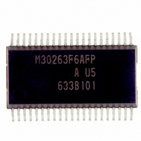
M30263F6AFP#U5A Renesas Electronics America, M30263F6AFP#U5A Datasheet - Page 126

M30263F6AFP#U5A
Manufacturer Part Number
M30263F6AFP#U5A
Description
IC M16C/26A MCU FLASH 42-SSOP
Manufacturer
Renesas Electronics America
Series
M16C™ M16C/Tiny/26r
Datasheet
1.M30260F3AGPU5A.pdf
(354 pages)
Specifications of M30263F6AFP#U5A
Core Processor
M16C/60
Core Size
16-Bit
Speed
20MHz
Connectivity
I²C, IEBus, SIO, UART/USART
Peripherals
DMA, PWM, Voltage Detect, WDT
Number Of I /o
33
Program Memory Size
48KB (48K x 8)
Program Memory Type
FLASH
Ram Size
2K x 8
Voltage - Supply (vcc/vdd)
2.7 V ~ 5.5 V
Data Converters
A/D 10x10b
Oscillator Type
Internal
Operating Temperature
-20°C ~ 85°C
Package / Case
42-SSOP
For Use With
R0K33026AS000BE - KIT DEV EVALUATION M16C/26A
Lead Free Status / RoHS Status
Lead free / RoHS Compliant
Eeprom Size
-
- Current page: 126 of 354
- Download datasheet (4Mb)
R
R
M
e
E
1
. v
J
Figure 12.1.4.2. Example of 16-bit Pulse Width Modulator Operation
Figure 12.1.4.3. Example of 8-bit Pulse Width Modulator Operation
6
0
C
2
9
0 .
B
2 /
0
0
6
2
A
0
F
f
i = 0 to 4
Count source
Input signal to
TA
Underflow signal of
8-bit prescaler
PWM pulse output
from TA
IR bit in the
TAiIC register
2
NOTES:
j
e
: Frequency of count source
G
0 -
b
iIN
1. The 8-bit prescaler counts the count source.
2. The 8-bit pulse width modulator counts the 8-bit prescaler's underflow signal.
3. m = 00
4. This timing diagram is for the case where the TAi register is set to "0202
(f
1 .
o r
2
1
0
ONSF or TRGSR register is set to "00
edge), and the MR2 bit in the TAiMR register is set to "1" (trigger selected by TAiTGH and TAiTGL bits).
pin
, 5
, f
u
0
p
2
iOUT
NOTES:
2
f
i = 0 to 4
, f
j
IR bit in the
TAiIC register
Count source
Input signal to
TA
PWM pulse output
from TA
: Frequency of count source
0
(
8
1. n = 0000
2. This timing diagram is for the case where the TAi register is set to "0003
M
, f
0
(f
iIN
16
pin
the ONSF or TRGSR register is set to "00
(rising edge), and the MR2 bit in the TAiMR register is set to "1" (trigger selected by TAiTGH and TAiTGL bits).
7
1
32
1
(1)
, f
pin
(2)
to FF
6
, f
2
iOUT
, f
page 107
C
C32
8
2 /
, f
16
)
16
pin
32
6
; n = 00
, f
, A
to FFFE
“H”
“L”
“H”
“L”
“H”
“L”
“1”
“0”
C32
M
)
“H”
“L”
“H”
“L”
“1”
“0”
1
f o
16
16
6
.
C
3
to FE
2
2 /
9
6
16
, B
.
M
2
" (TAi
1
Set to “0” upon accepting an interrupt request or by writing in program
6
Set to “0” upon accepting an interrupt request or by writing in program
C
2
2 /
IN
" (TAi
6
pin input), the MR1 bit in the TAiMR register is set to "0"(falling
Trigger is not generated by this signal
) T
IN
1 / f
1 / f
1 / f
pin input), the MR1 bit in the TAiMR register is set to "1"
i
j
X
j
1 / f
X
X (m + 1)
(2
1 / f
n
16
j
j
– 1)
X (m + 1) X (2 – 1)
X (m + 1) X n
16
16
", the TAiTGH and TAiTGL bits in
", the TAiTGH and TAiTGL bits in the
8
12. Timer
Related parts for M30263F6AFP#U5A
Image
Part Number
Description
Manufacturer
Datasheet
Request
R

Part Number:
Description:
KIT STARTER FOR M16C/29
Manufacturer:
Renesas Electronics America
Datasheet:

Part Number:
Description:
KIT STARTER FOR R8C/2D
Manufacturer:
Renesas Electronics America
Datasheet:

Part Number:
Description:
R0K33062P STARTER KIT
Manufacturer:
Renesas Electronics America
Datasheet:

Part Number:
Description:
KIT STARTER FOR R8C/23 E8A
Manufacturer:
Renesas Electronics America
Datasheet:

Part Number:
Description:
KIT STARTER FOR R8C/25
Manufacturer:
Renesas Electronics America
Datasheet:

Part Number:
Description:
KIT STARTER H8S2456 SHARPE DSPLY
Manufacturer:
Renesas Electronics America
Datasheet:

Part Number:
Description:
KIT STARTER FOR R8C38C
Manufacturer:
Renesas Electronics America
Datasheet:

Part Number:
Description:
KIT STARTER FOR R8C35C
Manufacturer:
Renesas Electronics America
Datasheet:

Part Number:
Description:
KIT STARTER FOR R8CL3AC+LCD APPS
Manufacturer:
Renesas Electronics America
Datasheet:

Part Number:
Description:
KIT STARTER FOR RX610
Manufacturer:
Renesas Electronics America
Datasheet:

Part Number:
Description:
KIT STARTER FOR R32C/118
Manufacturer:
Renesas Electronics America
Datasheet:

Part Number:
Description:
KIT DEV RSK-R8C/26-29
Manufacturer:
Renesas Electronics America
Datasheet:

Part Number:
Description:
KIT STARTER FOR SH7124
Manufacturer:
Renesas Electronics America
Datasheet:

Part Number:
Description:
KIT STARTER FOR H8SX/1622
Manufacturer:
Renesas Electronics America
Datasheet:

Part Number:
Description:
KIT DEV FOR SH7203
Manufacturer:
Renesas Electronics America
Datasheet:


