M30263F6AFP#U5A Renesas Electronics America, M30263F6AFP#U5A Datasheet - Page 79
M30263F6AFP#U5A
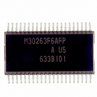
Manufacturer Part Number
M30263F6AFP#U5A
Description
IC M16C/26A MCU FLASH 42-SSOP
Manufacturer
Renesas Electronics America
Series
M16C™ M16C/Tiny/26r
Datasheet
1.M30260F3AGPU5A.pdf
(354 pages)
Specifications of M30263F6AFP#U5A
Core Processor
M16C/60
Core Size
16-Bit
Speed
20MHz
Connectivity
I²C, IEBus, SIO, UART/USART
Peripherals
DMA, PWM, Voltage Detect, WDT
Number Of I /o
33
Program Memory Size
48KB (48K x 8)
Program Memory Type
FLASH
Ram Size
2K x 8
Voltage - Supply (vcc/vdd)
2.7 V ~ 5.5 V
Data Converters
A/D 10x10b
Oscillator Type
Internal
Operating Temperature
-20°C ~ 85°C
Package / Case
42-SSOP
For Use With
R0K33026AS000BE - KIT DEV EVALUATION M16C/26A
Lead Free Status / RoHS Status
Lead free / RoHS Compliant
Eeprom Size
-


R
R
M
e
E
8. Protection
. v
J
1
Figure 8.1. PRCR Register
0
6
2
9
In the event that a program runs out of control, this function protects the important registers so that they will
not be rewritten easily. Figure 8.1 shows the PRCR register. The following lists the registers protected by
the PRCR register.
Set the PRC2 bit to “1” (write enabled) and then write to SFR area, and the PRC2 bit will be cleared to “0”
(write protected). The registers protected by the PRC2 bit should be changed in the next instruction after
setting the PRC2 bit to “1”. Make sure no interrupts or DMA transfers will occur between the instruction in
which the PRC2 bit is set to “1” and the next instruction. The PRC0, PRC1 and PRC3 bits are not automati-
cally cleared to “0” by writing to any address. They can only be cleared in a program.
C
0 .
B
2 /
Note
0
0
• Registers protected by PRC0 bit: CM0, CM1, CM2, PLC0, ROCR and PCLKR registers
• Registers protected by PRC1 bit: PM0, PM1, PM2, TB2SC, INVC0 and INVC1 registers
• Registers protected by PRC2 bit: PD9, PACR and NDDR registers
• Registers protected by PRC3 bit: VCR2 and D4INT registers
2
6
0
NOTE:
F
Protect register
A
b7
2
e
0 -
G
1. The PRC2 bit is set to "0" if data is written to the SFR area after the PRC2 bit is set to "1". The
b
b6
1 .
The PRC3 bit in the PRCR register is not available in M16C/26T.
2
o r
PRC0, PRC1 and PRC3 bits are not automatically set to "0". Set them to "0" by program.
0
, 5
b5
0
0
u
p
2
b4
0
0
(
0
M
7
b3
1
6
b2
C
2 /
page 60
b1
6
, A
b0
M
Bit symbol
(b5-b4)
(b7-b6)
f o
1
PRC0
PRC1
PRC2
PRC3
6
Symbol
PRCR
3
C
2
2 /
9
6
, B
Nothing is assigned. When write, set to "0". When read, its
content is indeterminate.
M
Protect bit 0
Protect bit 1
Protect bit 2
Protect bit 3
Reserved bit
1
6
C
2 /
6
Bit name
Address
) T
000A
16
XX000000
After reset
Enable write to CM0, CM1, CM2,
ROCR, PLC0 and PCLKR registers
Enable write to PM0, PM1, PM2,
TB2SC, INVC0 and INVC1
registers
Enable write to PD9, PACR and
NDDR registers
Enable write to VCR2 and D4INT
registers
Must set to "0"
0 : Write protected
1 : Write enabled
0 : Write protected
1 : Write enabled
0 : Write protected
1 : Write enabled
0 : Write protected
1 : Write enabled
2
Function
RW
RW
RW
RW
RW
RW
8. Protection
Related parts for M30263F6AFP#U5A
Image
Part Number
Description
Manufacturer
Datasheet
Request
R

Part Number:
Description:
KIT STARTER FOR M16C/29
Manufacturer:
Renesas Electronics America
Datasheet:

Part Number:
Description:
KIT STARTER FOR R8C/2D
Manufacturer:
Renesas Electronics America
Datasheet:

Part Number:
Description:
R0K33062P STARTER KIT
Manufacturer:
Renesas Electronics America
Datasheet:

Part Number:
Description:
KIT STARTER FOR R8C/23 E8A
Manufacturer:
Renesas Electronics America
Datasheet:

Part Number:
Description:
KIT STARTER FOR R8C/25
Manufacturer:
Renesas Electronics America
Datasheet:

Part Number:
Description:
KIT STARTER H8S2456 SHARPE DSPLY
Manufacturer:
Renesas Electronics America
Datasheet:

Part Number:
Description:
KIT STARTER FOR R8C38C
Manufacturer:
Renesas Electronics America
Datasheet:

Part Number:
Description:
KIT STARTER FOR R8C35C
Manufacturer:
Renesas Electronics America
Datasheet:

Part Number:
Description:
KIT STARTER FOR R8CL3AC+LCD APPS
Manufacturer:
Renesas Electronics America
Datasheet:
Part Number:
Description:
KIT STARTER FOR RX610
Manufacturer:
Renesas Electronics America
Datasheet:

Part Number:
Description:
KIT STARTER FOR R32C/118
Manufacturer:
Renesas Electronics America
Datasheet:

Part Number:
Description:
KIT DEV RSK-R8C/26-29
Manufacturer:
Renesas Electronics America
Datasheet:

Part Number:
Description:
KIT STARTER FOR SH7124
Manufacturer:
Renesas Electronics America
Datasheet:

Part Number:
Description:
KIT STARTER FOR H8SX/1622
Manufacturer:
Renesas Electronics America
Datasheet:

Part Number:
Description:
KIT DEV FOR SH7203
Manufacturer:
Renesas Electronics America
Datasheet: