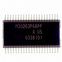
M30263F6AFP#U5A Renesas Electronics America, M30263F6AFP#U5A Datasheet - Page 251

M30263F6AFP#U5A
Manufacturer Part Number
M30263F6AFP#U5A
Description
IC M16C/26A MCU FLASH 42-SSOP
Manufacturer
Renesas Electronics America
Series
M16C™ M16C/Tiny/26r
Datasheet
1.M30260F3AGPU5A.pdf
(354 pages)
Specifications of M30263F6AFP#U5A
Core Processor
M16C/60
Core Size
16-Bit
Speed
20MHz
Connectivity
I²C, IEBus, SIO, UART/USART
Peripherals
DMA, PWM, Voltage Detect, WDT
Number Of I /o
33
Program Memory Size
48KB (48K x 8)
Program Memory Type
FLASH
Ram Size
2K x 8
Voltage - Supply (vcc/vdd)
2.7 V ~ 5.5 V
Data Converters
A/D 10x10b
Oscillator Type
Internal
Operating Temperature
-20°C ~ 85°C
Package / Case
42-SSOP
For Use With
R0K33026AS000BE - KIT DEV EVALUATION M16C/26A
Lead Free Status / RoHS Status
Lead free / RoHS Compliant
Eeprom Size
-
- Current page: 251 of 354
- Download datasheet (4Mb)
M
R
R
17.2 Memory Map
e
E
1
. v
J
6
Figure 17.2.1. Flash Memory Block Diagram (ROM capacity 64K byte)
0
C
The flash memory contains the user ROM area and the boot ROM area (reserved area). Figures 17.2.1 to
17.2.3 show the flash memory block diagram. The user ROM area has space to store the microcomputer
operation program in single-chip mode and a separate 2-Kbyte space as the block A and B.
The user ROM area is divided into several blocks. The user ROM area can be rewritten in CPU rewrite,
standard serial input/output, and parallel input/output modes. However, if block 0 and 1 are rewritten in
CPU rewrite mode, setting the FMR02 bit in the FMR0 register to “1” (block 0, 1 rewrite enabled) and the
FMR16 bit in the FMR1 register to “1”(blocks 0 to 3 rewrite enabled) enable rewriting. Also, if blocks 2 to 3
are rewritten in CPU rewrite mode, setting the FMR16 bit in the FMR1 register to “1” (blocks 0 to 3 rewrite
enabled) enables writing. Setting the PM10 bit in the PM1 register to “1”(data area access enabled) for
block A and B enables to use.
2
9
0 .
2 /
B
0
0
6
2
A
0 F 0 0 0 0
0 F 7 F F F
0 F 8 0 0 0
0 F B F F F
0 F C 0 0 0
0 F D F F F
0 F E 0 0 0
0 F F F F F
0 0 F 0 0 0
0 0 F 7 F F
0 0 F 8 0 0
0 0 F F F F
0
F
2
e
G
0 -
b
o r
1 .
2
1 6
1 6
1 6
1 6
1 6
0
u
1 6
1 6
1 6
1 6
1 6
1 6
, 5
1 6
0
p
2
(
0
M
B l o c k 3 : 3 2 K b y t e s (5)
B l o c k 2 : 1 6 K b y t e s (5)
0
B l o c k 1 : 8 K b y t e s (3)
B l o c k 0 : 8 K b y t e s (3)
B l o c k B : 2 K b y t e s (2)
B l o c k A : 2 K b y t e s (2)
1
7
6
B l o c k 2 : 1 6 K b y t e s
U s e r R O M a r e a
C
page 232
2 /
6
, A
M
1
f o
6
C
3
2
2 /
9
6
, B
M
1
6
C
2 /
NOTES:
6
) T
1. To specify a block, use the maximum even address in the block.
2. Blocks A and B are enabled to use when the PM10 bit in the PM1
3. Blocks 0 and 1 are enabled for programs and erases when the
4. The boot ROM area is reserved. Do not access.
5. Blocks 2 and 3 are enabled for programs and erases when the
register is set to "1".
FMR02 bit in the FMR0 register is set to "1" and the FMR16 bit in
the FMR1 register is set to "1". (CPU rewrite mode only)
FMR16 bit in the FMR1 register is set to "1". (CPU rewrite mode
only)
0 F F F F F
0 F F 0 0 0
1 6
1 6
B o o t R O M a r e a
4 K b y t e s (4)
17. Flash Memory Version
Related parts for M30263F6AFP#U5A
Image
Part Number
Description
Manufacturer
Datasheet
Request
R

Part Number:
Description:
KIT STARTER FOR M16C/29
Manufacturer:
Renesas Electronics America
Datasheet:

Part Number:
Description:
KIT STARTER FOR R8C/2D
Manufacturer:
Renesas Electronics America
Datasheet:

Part Number:
Description:
R0K33062P STARTER KIT
Manufacturer:
Renesas Electronics America
Datasheet:

Part Number:
Description:
KIT STARTER FOR R8C/23 E8A
Manufacturer:
Renesas Electronics America
Datasheet:

Part Number:
Description:
KIT STARTER FOR R8C/25
Manufacturer:
Renesas Electronics America
Datasheet:

Part Number:
Description:
KIT STARTER H8S2456 SHARPE DSPLY
Manufacturer:
Renesas Electronics America
Datasheet:

Part Number:
Description:
KIT STARTER FOR R8C38C
Manufacturer:
Renesas Electronics America
Datasheet:

Part Number:
Description:
KIT STARTER FOR R8C35C
Manufacturer:
Renesas Electronics America
Datasheet:

Part Number:
Description:
KIT STARTER FOR R8CL3AC+LCD APPS
Manufacturer:
Renesas Electronics America
Datasheet:

Part Number:
Description:
KIT STARTER FOR RX610
Manufacturer:
Renesas Electronics America
Datasheet:

Part Number:
Description:
KIT STARTER FOR R32C/118
Manufacturer:
Renesas Electronics America
Datasheet:

Part Number:
Description:
KIT DEV RSK-R8C/26-29
Manufacturer:
Renesas Electronics America
Datasheet:

Part Number:
Description:
KIT STARTER FOR SH7124
Manufacturer:
Renesas Electronics America
Datasheet:

Part Number:
Description:
KIT STARTER FOR H8SX/1622
Manufacturer:
Renesas Electronics America
Datasheet:

Part Number:
Description:
KIT DEV FOR SH7203
Manufacturer:
Renesas Electronics America
Datasheet:


