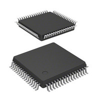
HD64F3694FPJV Renesas Electronics America, HD64F3694FPJV Datasheet - Page 287

HD64F3694FPJV
Manufacturer Part Number
HD64F3694FPJV
Description
MCU 3/5V 32K J-TEMP PB-FREE 64-L
Manufacturer
Renesas Electronics America
Series
H8® H8/300H Tinyr
Datasheet
1.HD64F3694GFYV.pdf
(452 pages)
Specifications of HD64F3694FPJV
Core Processor
H8/300H
Core Size
16-Bit
Speed
20MHz
Connectivity
I²C, SCI
Peripherals
PWM, WDT
Number Of I /o
29
Program Memory Size
32KB (32K x 8)
Program Memory Type
FLASH
Ram Size
2K x 8
Voltage - Supply (vcc/vdd)
3 V ~ 5.5 V
Data Converters
A/D 8x10b
Oscillator Type
Internal
Operating Temperature
-20°C ~ 75°C
Package / Case
64-LQFP
For Use With
R0K436079S000BE - KIT DEV FOR H8/36079 W/COMPILER
Lead Free Status / RoHS Status
Lead free / RoHS Compliant
Eeprom Size
-
- Current page: 287 of 452
- Download datasheet (3Mb)
15.4.7
The logic levels at the SCL and SDA pins are routed through noise cancelers before being latched
internally. Figure 15.16 shows a block diagram of the noise canceler circuit.
The noise canceler consists of two cascaded latches and a match detector. The SCL (or SDA)
input signal is sampled on the system clock, but is not passed forward to the next circuit unless the
outputs of both latches agree. If they do not agree, the previous value is held.
processing
ICDRS
ICDRR
RDRF
(Input)
MST
TRS
SCL
SDA
User
SCL or SDA
input signal
Sampling
clock
Noise Canceler
[2] Set MST
(when outputting the clock)
Bit 0
Figure 15.16 Block Diagram of Noise Conceler
1
Figure 15.15 Receive Mode Operation Timing
Sampling clock
D
System clock
Data 1
period
Latch
Bit 1
C
2
Q
Bit 6
D
7
Latch
[3] Read ICDRR
C
Bit 7
8
Q
Bit 0
Data 2
1
Data 1
Rev.5.00 Nov. 02, 2005 Page 257 of 418
March detector
Section 15 I
Bit 6
7
Bit 7
2
C Bus Interface 2 (IIC2)
8
SCL or SDA
Internal
REJ09B0028-0500
signal
1
[3] Read ICDRR
Data 2
Data 3
Bit 0
2
Related parts for HD64F3694FPJV
Image
Part Number
Description
Manufacturer
Datasheet
Request
R

Part Number:
Description:
KIT STARTER FOR M16C/29
Manufacturer:
Renesas Electronics America
Datasheet:

Part Number:
Description:
KIT STARTER FOR R8C/2D
Manufacturer:
Renesas Electronics America
Datasheet:

Part Number:
Description:
R0K33062P STARTER KIT
Manufacturer:
Renesas Electronics America
Datasheet:

Part Number:
Description:
KIT STARTER FOR R8C/23 E8A
Manufacturer:
Renesas Electronics America
Datasheet:

Part Number:
Description:
KIT STARTER FOR R8C/25
Manufacturer:
Renesas Electronics America
Datasheet:

Part Number:
Description:
KIT STARTER H8S2456 SHARPE DSPLY
Manufacturer:
Renesas Electronics America
Datasheet:

Part Number:
Description:
KIT STARTER FOR R8C38C
Manufacturer:
Renesas Electronics America
Datasheet:

Part Number:
Description:
KIT STARTER FOR R8C35C
Manufacturer:
Renesas Electronics America
Datasheet:

Part Number:
Description:
KIT STARTER FOR R8CL3AC+LCD APPS
Manufacturer:
Renesas Electronics America
Datasheet:

Part Number:
Description:
KIT STARTER FOR RX610
Manufacturer:
Renesas Electronics America
Datasheet:

Part Number:
Description:
KIT STARTER FOR R32C/118
Manufacturer:
Renesas Electronics America
Datasheet:

Part Number:
Description:
KIT DEV RSK-R8C/26-29
Manufacturer:
Renesas Electronics America
Datasheet:

Part Number:
Description:
KIT STARTER FOR SH7124
Manufacturer:
Renesas Electronics America
Datasheet:

Part Number:
Description:
KIT STARTER FOR H8SX/1622
Manufacturer:
Renesas Electronics America
Datasheet:


