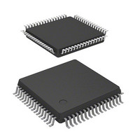
HD64F3694FPJV Renesas Electronics America, HD64F3694FPJV Datasheet - Page 441

HD64F3694FPJV
Manufacturer Part Number
HD64F3694FPJV
Description
MCU 3/5V 32K J-TEMP PB-FREE 64-L
Manufacturer
Renesas Electronics America
Series
H8® H8/300H Tinyr
Datasheet
1.HD64F3694GFYV.pdf
(452 pages)
Specifications of HD64F3694FPJV
Core Processor
H8/300H
Core Size
16-Bit
Speed
20MHz
Connectivity
I²C, SCI
Peripherals
PWM, WDT
Number Of I /o
29
Program Memory Size
32KB (32K x 8)
Program Memory Type
FLASH
Ram Size
2K x 8
Voltage - Supply (vcc/vdd)
3 V ~ 5.5 V
Data Converters
A/D 8x10b
Oscillator Type
Internal
Operating Temperature
-20°C ~ 75°C
Package / Case
64-LQFP
For Use With
R0K436079S000BE - KIT DEV FOR H8/36079 W/COMPILER
Lead Free Status / RoHS Status
Lead free / RoHS Compliant
Eeprom Size
-
- Current page: 441 of 452
- Download datasheet (3Mb)
Item
Preface
Section 1 Overview
Figure 1.1 Internal Block
Diagram of H8/3694
Group of F-ZTAT
and Mask-ROM Versions,
Figure 1.2 Internal Block
Diagram of H8/3694N
(EEPROM Stacked
Version)
Main Revisions and Additions in this Edition
TM
Page Revision (See Manual for Details)
vi, vii
4, 5
Notes:
When using the on-chip emulator (E7, E8) for H8/3694 program
development and debugging, the following restrictions must be
noted.
1. The NMI pin is reserved for the E7 or E8, and cannot be
3. Area H'7000 to H'7FFF is used by the E7 or E8, and is not
5. When the E7 or E8 is used, address breaks can be set as
6. When the E7 or E8 is used, NMI is an input/output pin
Note has been deleted.
used.
available to the user.
either available to the user or for use by the E7 or E8. If
address breaks are set as being used by the E7 or E8, the
address break control registers must not be accessed.
(open-drain in output mode), P85 and P87 are input pins,
and P86 is an output pin.
converter
Timer V
Data bus (upper)
A/D
Address bus
POR/LVD
(optional)
IIC2
Rev.5.00 Nov. 02, 2005 Page 411 of 418
REJ09B0028-0500
PB0/AN0
PB1/AN1
PB2/AN2
PB3/AN3
PB4/AN4
PB5/AN5
PB6/AN6
PB7/AN7
AV
CC
Related parts for HD64F3694FPJV
Image
Part Number
Description
Manufacturer
Datasheet
Request
R

Part Number:
Description:
KIT STARTER FOR M16C/29
Manufacturer:
Renesas Electronics America
Datasheet:

Part Number:
Description:
KIT STARTER FOR R8C/2D
Manufacturer:
Renesas Electronics America
Datasheet:

Part Number:
Description:
R0K33062P STARTER KIT
Manufacturer:
Renesas Electronics America
Datasheet:

Part Number:
Description:
KIT STARTER FOR R8C/23 E8A
Manufacturer:
Renesas Electronics America
Datasheet:

Part Number:
Description:
KIT STARTER FOR R8C/25
Manufacturer:
Renesas Electronics America
Datasheet:

Part Number:
Description:
KIT STARTER H8S2456 SHARPE DSPLY
Manufacturer:
Renesas Electronics America
Datasheet:

Part Number:
Description:
KIT STARTER FOR R8C38C
Manufacturer:
Renesas Electronics America
Datasheet:

Part Number:
Description:
KIT STARTER FOR R8C35C
Manufacturer:
Renesas Electronics America
Datasheet:

Part Number:
Description:
KIT STARTER FOR R8CL3AC+LCD APPS
Manufacturer:
Renesas Electronics America
Datasheet:

Part Number:
Description:
KIT STARTER FOR RX610
Manufacturer:
Renesas Electronics America
Datasheet:

Part Number:
Description:
KIT STARTER FOR R32C/118
Manufacturer:
Renesas Electronics America
Datasheet:

Part Number:
Description:
KIT DEV RSK-R8C/26-29
Manufacturer:
Renesas Electronics America
Datasheet:

Part Number:
Description:
KIT STARTER FOR SH7124
Manufacturer:
Renesas Electronics America
Datasheet:

Part Number:
Description:
KIT STARTER FOR H8SX/1622
Manufacturer:
Renesas Electronics America
Datasheet:


