MC908AZ60AVFUER Freescale Semiconductor, MC908AZ60AVFUER Datasheet - Page 168
MC908AZ60AVFUER
Manufacturer Part Number
MC908AZ60AVFUER
Description
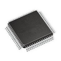
IC MCU 64K FLASH 8.4MHZ 64-QFP
Manufacturer
Freescale Semiconductor
Series
HC08r
Datasheet
1.MC908AZ60ACFUER.pdf
(414 pages)
Specifications of MC908AZ60AVFUER
Core Processor
HC08
Core Size
8-Bit
Speed
8.4MHz
Connectivity
CAN, SCI, SPI
Peripherals
LVD, POR, PWM
Number Of I /o
52
Program Memory Size
60KB (60K x 8)
Program Memory Type
FLASH
Eeprom Size
1K x 8
Ram Size
2K x 8
Voltage - Supply (vcc/vdd)
4.5 V ~ 5.5 V
Data Converters
A/D 15x8b
Oscillator Type
Internal
Operating Temperature
-40°C ~ 105°C
Package / Case
64-QFP
Processor Series
HC08AZ
Core
HC08
Data Bus Width
8 bit
Data Ram Size
2 KB
Interface Type
SCI, SPI
Maximum Clock Frequency
8.4 MHz
Number Of Programmable I/os
52
Number Of Timers
8
Maximum Operating Temperature
+ 105 C
Mounting Style
SMD/SMT
Development Tools By Supplier
FSICEBASE, M68CBL05CE, ZK-HC08AX-A, M68EM08AS/AZ60AE
Minimum Operating Temperature
- 40 C
On-chip Adc
8 bit, 15 Channel
Lead Free Status / RoHS Status
Lead free / RoHS Compliant
Available stocks
Company
Part Number
Manufacturer
Quantity
Price
Company:

Part Number:
MC908AZ60AVFUER
Manufacturer:
Freescale Semiconductor
Quantity:
10 000


Low-Voltage Inhibit (LVI)
16.3.1 Polled LVI Operation
In applications that can operate at V
polling the LVIOUT bit. In the configuration register, the LVIPWR bit must be at logic 1 to enable the LVI
module, and the LVIRST bit must be at logic 0 to disable LVI resets.
16.3.2 Forced Reset Operation
In applications that require V
module to reset the MCU when V
or more consecutive CPU cycles. In the configuration register, the LVIPWR and LVIRST bits must be at
logic 1 to enable the LVI module and to enable LVI resets.
16.3.3 False Reset Protection
The V
module to reset the MCU,V
CPU cycles. V
168
$FE0F
Addr.
DD
pin level is digitally filtered to reduce false resets due to power supply noise. In order for the LVI
DETECTOR
LVI Status Register (LVISR)
LOW V
DD
Register Name
V
DD
MC68HC908AZ60A • MC68HC908AS60A • MC68HC908AS60E Data Sheet, Rev. 6
must be above LVI
DD
V
V
DD
DD
> LVI
< LVI
DD
DD
TRIP
CPU CLOCK
TRIP
must remain at or below the LVI
Figure 16-1. LVI Module Block Diagram
Figure 16-2. LVI I/O Register Summary
= 0
= 1
to remain above the LVI
ANLGTRIP
FROM CONFIG-1
DD
Read: LVIOUT
Write:
LVIPWR
DD
falls to the LVI
TRIPR
levels below the LVI
Bit 7
DIGITAL FILTER
FROM CONFIG-1
Filter Bypass
Stop Mode
for only one CPU cycle to bring the MCU out of reset.
LVISTOP
V
DD
= Unimplemented
6
0
TRIPF
LVIOUT
TRIPF
level and remains at or below that level for nine
5
0
TRIPF
level, enabling LVI resets allows the LVI
TRIPF
FROM CONFIG-1
level, software can monitor V
LVIRST
4
0
level for nine or more consecutive
3
0
2
0
Freescale Semiconductor
LVI RESET
1
0
DD
by
Bit 0
0
Related parts for MC908AZ60AVFUER
Image
Part Number
Description
Manufacturer
Datasheet
Request
R

Part Number:
Description:
Manufacturer:
Freescale Semiconductor, Inc
Datasheet:
Part Number:
Description:
Manufacturer:
Freescale Semiconductor, Inc
Datasheet:
Part Number:
Description:
Manufacturer:
Freescale Semiconductor, Inc
Datasheet:
Part Number:
Description:
Manufacturer:
Freescale Semiconductor, Inc
Datasheet:
Part Number:
Description:
Manufacturer:
Freescale Semiconductor, Inc
Datasheet:
Part Number:
Description:
Manufacturer:
Freescale Semiconductor, Inc
Datasheet:
Part Number:
Description:
Manufacturer:
Freescale Semiconductor, Inc
Datasheet:
Part Number:
Description:
Manufacturer:
Freescale Semiconductor, Inc
Datasheet:
Part Number:
Description:
Manufacturer:
Freescale Semiconductor, Inc
Datasheet:
Part Number:
Description:
Manufacturer:
Freescale Semiconductor, Inc
Datasheet:
Part Number:
Description:
Manufacturer:
Freescale Semiconductor, Inc
Datasheet:
Part Number:
Description:
Manufacturer:
Freescale Semiconductor, Inc
Datasheet:
Part Number:
Description:
Manufacturer:
Freescale Semiconductor, Inc
Datasheet:
Part Number:
Description:
Manufacturer:
Freescale Semiconductor, Inc
Datasheet:
Part Number:
Description:
Manufacturer:
Freescale Semiconductor, Inc
Datasheet: