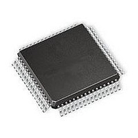
MC908AZ60AVFUER Freescale Semiconductor, MC908AZ60AVFUER Datasheet - Page 258

MC908AZ60AVFUER
Manufacturer Part Number
MC908AZ60AVFUER
Description
IC MCU 64K FLASH 8.4MHZ 64-QFP
Manufacturer
Freescale Semiconductor
Series
HC08r
Datasheet
1.MC908AZ60ACFUER.pdf
(414 pages)
Specifications of MC908AZ60AVFUER
Core Processor
HC08
Core Size
8-Bit
Speed
8.4MHz
Connectivity
CAN, SCI, SPI
Peripherals
LVD, POR, PWM
Number Of I /o
52
Program Memory Size
60KB (60K x 8)
Program Memory Type
FLASH
Eeprom Size
1K x 8
Ram Size
2K x 8
Voltage - Supply (vcc/vdd)
4.5 V ~ 5.5 V
Data Converters
A/D 15x8b
Oscillator Type
Internal
Operating Temperature
-40°C ~ 105°C
Package / Case
64-QFP
Processor Series
HC08AZ
Core
HC08
Data Bus Width
8 bit
Data Ram Size
2 KB
Interface Type
SCI, SPI
Maximum Clock Frequency
8.4 MHz
Number Of Programmable I/os
52
Number Of Timers
8
Maximum Operating Temperature
+ 105 C
Mounting Style
SMD/SMT
Development Tools By Supplier
FSICEBASE, M68CBL05CE, ZK-HC08AX-A, M68EM08AS/AZ60AE
Minimum Operating Temperature
- 40 C
On-chip Adc
8 bit, 15 Channel
Lead Free Status / RoHS Status
Lead free / RoHS Compliant
Available stocks
Company
Part Number
Manufacturer
Quantity
Price
Company:
Part Number:
MC908AZ60AVFUER
Manufacturer:
Freescale Semiconductor
Quantity:
10 000
- Current page: 258 of 414
- Download datasheet (5Mb)
Input/Output Ports
22.6 Port E
Port E is an 8-bit special function port that shares two of its pins with the timer interface module (TIMA),
two of its pins with the serial communications interface module (SCI), and four of its pins with the serial
peripheral interface module (SPI).
22.6.1 Port E Data Register
The port E data register contains a data latch for each of the eight port E pins.
PTE[7:0] — Port E Data Bits
SPSCK — SPI Serial Clock Bit
MOSI — Master Out/Slave In Bit
MISO — Master In/Slave Out Bit
SS — Slave Select Bit
258
PTE[7:0] are read/write, software programmable bits. Data direction of each port E pin is under the
control of the corresponding bit in data direction register E.
The PTE7/SPSCK pin is the serial clock input of an SPI slave module and serial clock output of an SPI
master module. When the SPE bit is clear, the PTE7/SPSCK pin is available for general-purpose I/O.
(See
The PTE6/MOSI pin is the master out/slave in terminal of the SPI module. When the SPE bit is clear,
the PTE6/MOSI pin is available for general-purpose I/O.
The PTE5/MISO pin is the master in/slave out terminal of the SPI module. When the SPI enable bit,
SPE, is clear, the SPI module is disabled, and the PTE5/MISO pin is available for general-purpose I/O.
(See
The PTE4/SS pin is the slave select input of the SPI module. When the SPE bit is clear, or when the
SPI master bit, SPMSTR, is set and MODFEN bit is low, the PTE4/SS pin is available for
general-purpose I/O. (See
bit in data direction register E (DDRE) has no effect on the PTE4/SS pin.
19.13.1 SPI Control
19.13.1 SPI Control
Alternative
Function:
Address:
Data direction register E (DDRE) does not affect the data direction of port
E pins that are being used by the SPI module. However, the DDRE bits
always determine whether reading port E returns the states of the latches
or the states of the pins. (See
Reset:
Read:
Write:
MC68HC908AZ60A • MC68HC908AS60A • MC68HC908AS60E Data Sheet, Rev. 6
SPSCK
$0008
PTE7
Bit 7
Register).
Register).
19.12.4 SS (Slave
Figure 22-14. Port E Data Register (PTE)
PTE6
MOSI
6
PTE5
MISO
5
Table
Select)). When the SPI is enabled as a slave, the DDRF0
NOTE
Unaffected by Reset
PTE4
SS
22-5).
4
TACH1
PTE3
3
TACH0
PTE2
2
PTE1
RxD
1
Freescale Semiconductor
PTE0
Bit 0
TxD
Related parts for MC908AZ60AVFUER
Image
Part Number
Description
Manufacturer
Datasheet
Request
R
Part Number:
Description:
Manufacturer:
Freescale Semiconductor, Inc
Datasheet:
Part Number:
Description:
Manufacturer:
Freescale Semiconductor, Inc
Datasheet:
Part Number:
Description:
Manufacturer:
Freescale Semiconductor, Inc
Datasheet:
Part Number:
Description:
Manufacturer:
Freescale Semiconductor, Inc
Datasheet:
Part Number:
Description:
Manufacturer:
Freescale Semiconductor, Inc
Datasheet:
Part Number:
Description:
Manufacturer:
Freescale Semiconductor, Inc
Datasheet:
Part Number:
Description:
Manufacturer:
Freescale Semiconductor, Inc
Datasheet:
Part Number:
Description:
Manufacturer:
Freescale Semiconductor, Inc
Datasheet:
Part Number:
Description:
Manufacturer:
Freescale Semiconductor, Inc
Datasheet:
Part Number:
Description:
Manufacturer:
Freescale Semiconductor, Inc
Datasheet:
Part Number:
Description:
Manufacturer:
Freescale Semiconductor, Inc
Datasheet:
Part Number:
Description:
Manufacturer:
Freescale Semiconductor, Inc
Datasheet:
Part Number:
Description:
Manufacturer:
Freescale Semiconductor, Inc
Datasheet:
Part Number:
Description:
Manufacturer:
Freescale Semiconductor, Inc
Datasheet:
Part Number:
Description:
Manufacturer:
Freescale Semiconductor, Inc
Datasheet:


