MC908AZ60AVFUER Freescale Semiconductor, MC908AZ60AVFUER Datasheet - Page 362
MC908AZ60AVFUER
Manufacturer Part Number
MC908AZ60AVFUER
Description
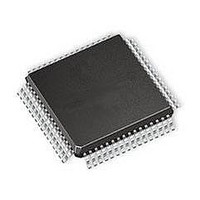
IC MCU 64K FLASH 8.4MHZ 64-QFP
Manufacturer
Freescale Semiconductor
Series
HC08r
Datasheet
1.MC908AZ60ACFUER.pdf
(414 pages)
Specifications of MC908AZ60AVFUER
Core Processor
HC08
Core Size
8-Bit
Speed
8.4MHz
Connectivity
CAN, SCI, SPI
Peripherals
LVD, POR, PWM
Number Of I /o
52
Program Memory Size
60KB (60K x 8)
Program Memory Type
FLASH
Eeprom Size
1K x 8
Ram Size
2K x 8
Voltage - Supply (vcc/vdd)
4.5 V ~ 5.5 V
Data Converters
A/D 15x8b
Oscillator Type
Internal
Operating Temperature
-40°C ~ 105°C
Package / Case
64-QFP
Processor Series
HC08AZ
Core
HC08
Data Bus Width
8 bit
Data Ram Size
2 KB
Interface Type
SCI, SPI
Maximum Clock Frequency
8.4 MHz
Number Of Programmable I/os
52
Number Of Timers
8
Maximum Operating Temperature
+ 105 C
Mounting Style
SMD/SMT
Development Tools By Supplier
FSICEBASE, M68CBL05CE, ZK-HC08AX-A, M68EM08AS/AZ60AE
Minimum Operating Temperature
- 40 C
On-chip Adc
8 bit, 15 Channel
Lead Free Status / RoHS Status
Lead free / RoHS Compliant
Available stocks
Company
Part Number
Manufacturer
Quantity
Price
Company:

Part Number:
MC908AZ60AVFUER
Manufacturer:
Freescale Semiconductor
Quantity:
10 000


Byte Data Link Controller (BDLC)
Upon receiving a BDLC interrupt, the user can read the value within the BSVR, transferring it to the CPU’s
index register. The value can then be used to index into a jump table, with entries four bytes apart, to
quickly enter the appropriate service routine. For example:
The service routines should clear all of the sources that are causing the pending interrupts. Note that the
clearing of a high priority interrupt may still leave a lower priority interrupt pending, in which case bits I0,
I1, and I2 of the BSVR will then reflect the source of the remaining interrupt request.
If fewer states are used or if a different software approach is taken, the jump table can be made smaller
or omitted altogether.
27.6.5 BDLC Data Register
This register is used to pass the data to be transmitted to the J1850 bus from the CPU to the BDLC. It is
also used to pass data received from the J1850 bus to the CPU. Each data byte (after the first one) should
be written only after a Tx data register empty (TDRE) state is indicated in the BSVR.
Data read from this register will be the last data byte received from the J1850 bus. This received data
should only be read after an Rx data register full (RDRF) interrupt has occurred. (See
Vector
362
Register)
Service
*
*
JMPTAB
*
Address:
The NOPs are used only to align the JMPs onto 4-byte boundaries so that
the value in the BSVR can be used intact. Each of the service routines must
end with an RTI instruction to guarantee correct continued operation of the
device. Note also that the first entry can be omitted since it corresponds to
no interrupt occurring.
Reset:
Read:
Write:
MC68HC908AZ60A • MC68HC908AS60A • MC68HC908AS60E Data Sheet, Rev. 6
$003F
Bit 7
D7
LDX
JMP
JMP
NOP
JMP
NOP
JMP
NOP
JMP
END
Figure 27-20. BDLC Data Register (BDR)
D6
6
BSVR
JMPTAB,X
SERVE0
SERVE1
SERVE2
SERVE8
D5
5
NOTE
Unaffected by Reset
Fetch State Vector Number
Enter service routine,
(must end in RTI)
Service condition #0
Service condition #1
Service condition #2
Service condition #8
D4
4
D3
3
D2
2
D1
1
Freescale Semiconductor
27.6.4 BDLC State
Bit 0
D0
Related parts for MC908AZ60AVFUER
Image
Part Number
Description
Manufacturer
Datasheet
Request
R

Part Number:
Description:
Manufacturer:
Freescale Semiconductor, Inc
Datasheet:
Part Number:
Description:
Manufacturer:
Freescale Semiconductor, Inc
Datasheet:
Part Number:
Description:
Manufacturer:
Freescale Semiconductor, Inc
Datasheet:
Part Number:
Description:
Manufacturer:
Freescale Semiconductor, Inc
Datasheet:
Part Number:
Description:
Manufacturer:
Freescale Semiconductor, Inc
Datasheet:
Part Number:
Description:
Manufacturer:
Freescale Semiconductor, Inc
Datasheet:
Part Number:
Description:
Manufacturer:
Freescale Semiconductor, Inc
Datasheet:
Part Number:
Description:
Manufacturer:
Freescale Semiconductor, Inc
Datasheet:
Part Number:
Description:
Manufacturer:
Freescale Semiconductor, Inc
Datasheet:
Part Number:
Description:
Manufacturer:
Freescale Semiconductor, Inc
Datasheet:
Part Number:
Description:
Manufacturer:
Freescale Semiconductor, Inc
Datasheet:
Part Number:
Description:
Manufacturer:
Freescale Semiconductor, Inc
Datasheet:
Part Number:
Description:
Manufacturer:
Freescale Semiconductor, Inc
Datasheet:
Part Number:
Description:
Manufacturer:
Freescale Semiconductor, Inc
Datasheet:
Part Number:
Description:
Manufacturer:
Freescale Semiconductor, Inc
Datasheet: