D12363VF33V Renesas Electronics America, D12363VF33V Datasheet - Page 227
D12363VF33V
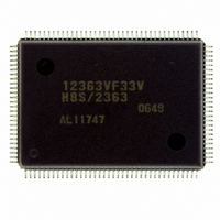
Manufacturer Part Number
D12363VF33V
Description
IC H8S/2363 MCU ROMLESS 128QFP
Manufacturer
Renesas Electronics America
Series
H8® H8S/2300r
Specifications of D12363VF33V
Core Processor
H8S/2000
Core Size
16-Bit
Speed
33MHz
Connectivity
I²C, IrDA, SCI, SmartCard
Peripherals
DMA, POR, PWM, WDT
Number Of I /o
84
Program Memory Type
ROMless
Ram Size
16K x 8
Voltage - Supply (vcc/vdd)
3 V ~ 3.6 V
Data Converters
A/D 10x10b, D/A 2x8b
Oscillator Type
Internal
Operating Temperature
-20°C ~ 75°C
Package / Case
128-QFP
For Use With
YR0K42378FC000BA - KIT EVAL FOR H8S/2378
Lead Free Status / RoHS Status
Lead free / RoHS Compliant
Eeprom Size
-
Program Memory Size
-
Available stocks
Company
Part Number
Manufacturer
Quantity
Price
Company:

Part Number:
D12363VF33V
Manufacturer:
ST
Quantity:
67 000
Company:
Part Number:
D12363VF33V
Manufacturer:
Renesas Electronics America
Quantity:
10 000
Part Number:
D12363VF33V
Manufacturer:
RENSAS
Quantity:
20 000


6.6.4
Table 6.6 shows the pins used for DRAM interfacing and their functions. Since the CS2, CS5 pins
are in the input state after a reset, set the corresponding DDR to 1 when RAS2, RAS5 signals are
output.
Table 6.6
Pin
HWR
CS2
CS3
UCAS
LCAS
RD, OE
WAIT
A15 to A0
D15 to D0
Pins Used for DRAM Interface
DRAM Interface Pins
With DRAM
Setting
WE
RAS2
RAS3
UCAS
LCAS
OE
WAIT
A15 to A0
D15 to D0
Name
Write enable
Row address strobe 2/
row address strobe
Row address strobe 3
Upper column address
strobe
Lower column address
strobe
Output enable
Wait
Address pins
Data pins
I/O
Output
Output
Output
Output
Output
Output
Input
Output
I/O
Rev.6.00 Mar. 18, 2009 Page 167 of 980
Function
Write enable for DRAM space
access
Row address strobe when area
2 is designated as DRAM space
or row address strobe when
areas 2 to 5 are designated as
continuous DRAM space
Row address strobe when area
3 is designated as DRAM space
Upper column address strobe for
16-bit DRAM space access or
column address strobe for 8-bit
DRAM space access
Lower column address strobe
signal for 16-bit DRAM space
access
Output enable signal for DRAM
space access
Wait request signal
Row address/column address
multiplexed output
Data input/output pins
Section 6 Bus Controller (BSC)
REJ09B0050-0600
Related parts for D12363VF33V
Image
Part Number
Description
Manufacturer
Datasheet
Request
R

Part Number:
Description:
KIT STARTER FOR M16C/29
Manufacturer:
Renesas Electronics America
Datasheet:

Part Number:
Description:
KIT STARTER FOR R8C/2D
Manufacturer:
Renesas Electronics America
Datasheet:

Part Number:
Description:
R0K33062P STARTER KIT
Manufacturer:
Renesas Electronics America
Datasheet:

Part Number:
Description:
KIT STARTER FOR R8C/23 E8A
Manufacturer:
Renesas Electronics America
Datasheet:

Part Number:
Description:
KIT STARTER FOR R8C/25
Manufacturer:
Renesas Electronics America
Datasheet:

Part Number:
Description:
KIT STARTER H8S2456 SHARPE DSPLY
Manufacturer:
Renesas Electronics America
Datasheet:

Part Number:
Description:
KIT STARTER FOR R8C38C
Manufacturer:
Renesas Electronics America
Datasheet:

Part Number:
Description:
KIT STARTER FOR R8C35C
Manufacturer:
Renesas Electronics America
Datasheet:

Part Number:
Description:
KIT STARTER FOR R8CL3AC+LCD APPS
Manufacturer:
Renesas Electronics America
Datasheet:
Part Number:
Description:
KIT STARTER FOR RX610
Manufacturer:
Renesas Electronics America
Datasheet:

Part Number:
Description:
KIT STARTER FOR R32C/118
Manufacturer:
Renesas Electronics America
Datasheet:

Part Number:
Description:
KIT DEV RSK-R8C/26-29
Manufacturer:
Renesas Electronics America
Datasheet:

Part Number:
Description:
KIT STARTER FOR SH7124
Manufacturer:
Renesas Electronics America
Datasheet:

Part Number:
Description:
KIT STARTER FOR H8SX/1622
Manufacturer:
Renesas Electronics America
Datasheet:

Part Number:
Description:
KIT DEV FOR SH7203
Manufacturer:
Renesas Electronics America
Datasheet: